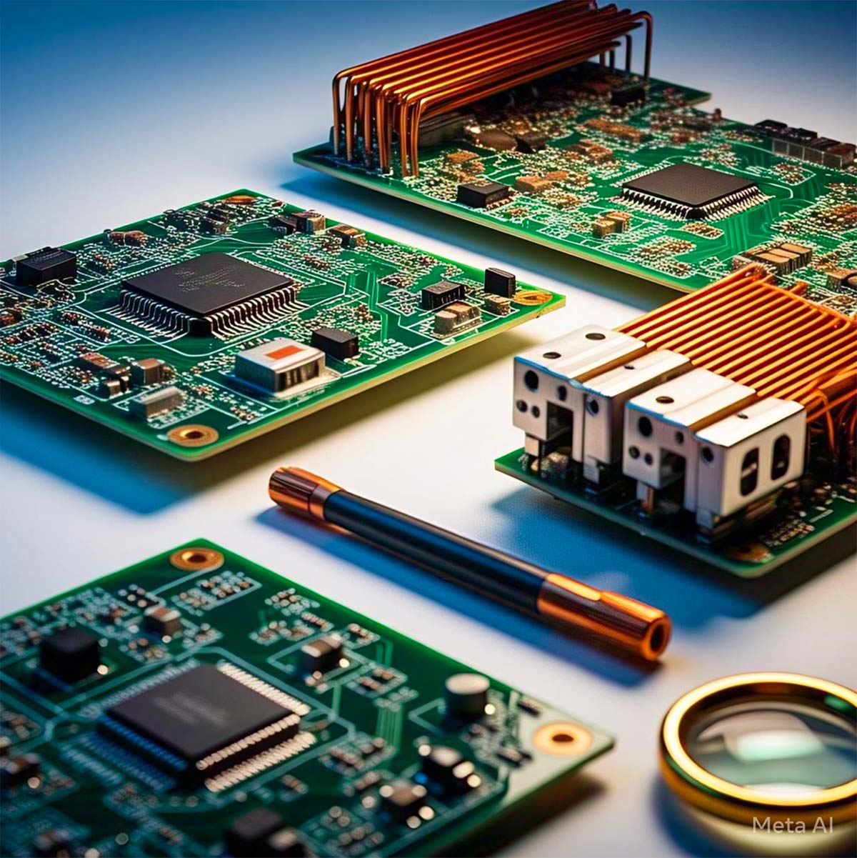
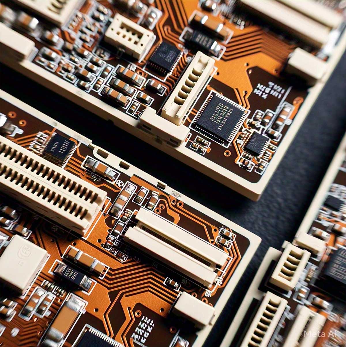
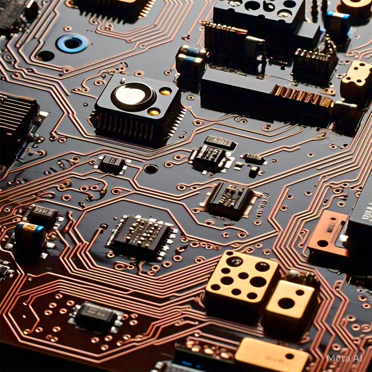
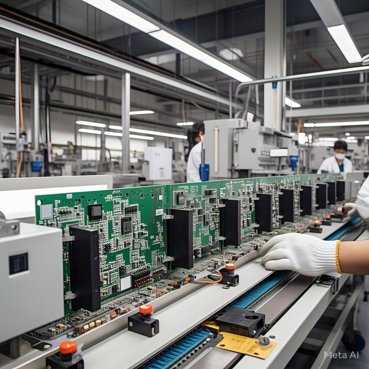
Below is a step-by-step overview of how PCBs are manufactured.
The invention and widespread adoption of printed circuit boards (PCBs) fundamentally transformed the electronics industry, enabling the compact, reliable, and scalable design of modern electronic devices. Before PCBs, electronics relied on point-to-point wiring, a labor-intensive and error-prone method that severely limited complexity and reliability. With PCBs, conductive pathways could be etched directly onto a non-conductive substrate, allowing components to be precisely arranged and permanently soldered into place. This innovation not only reduced the size and cost of electronic products but also dramatically improved their consistency and performance. From consumer gadgets and medical equipment to aerospace systems and industrial controls, PCBs have become the structural and electrical backbone of nearly every electronic device.
The manufacturing of PCBs, however, is far from simple. It involves a highly refined sequence of complex, tightly controlled steps, often performed in cleanroom environments to ensure precision and reliability. The process typically begins with the design of the circuit layout using specialized software, followed by the layering of copper and insulating materials. Photolithography, chemical etching, drilling, plating, and solder masking are just a few of the meticulous procedures required to produce a single PCB. Multilayer boards, common in advanced electronics, demand even greater accuracy and alignment across layers. Each phase must meet stringent quality standards to ensure signal integrity, mechanical durability, and thermal stability. The sophistication of PCB manufacturing reflects its critical role in enabling the miniaturization and complexity of today’s technology, serving as both a physical framework and a functional foundation for innovation.
1. PCB Design & Layout
Before manufacturing, engineers use PCB design software (such as Altium Designer, Eagle, or KiCad) to create a digital blueprint of the board. The design includes:
- Copper traces: Electrical connections between components.
- Pads & Vias: Connection points for components and inter-layer pathways.
- Silkscreen layer: Labels and markings for assembly.
- Drill holes: For through-hole components and vias.
Once finalized, the design is converted into Gerber files, which contain all the necessary fabrication details.
2. Substrate Preparation (Base Material Selection)
PCBs are typically made from FR4 (fiberglass-reinforced epoxy), CEM-3, or polyimide for flexible PCBs. The base material consists of:
- Substrate (FR4, etc.): Provides mechanical strength.
- Copper layer – Conductive layer for circuits.
- Solder mask layer – Insulating protection for copper traces.
- Silkscreen layer – Printed layer for component identification.
3. Printing Inner Layers (For Multilayer PCBs)
For multilayer PCBs, the inner copper layers are prepared using photoresist and etching processes:
- Photoresist Coating: A light-sensitive film is applied to the copper layer.
- UV Exposure: A mask with the circuit pattern is placed over the board and exposed to UV light. This hardens the exposed areas.
- Etching: Chemicals (such as ferric chloride or ammonium persulfate) remove unwanted copper, leaving behind the circuit pattern.
- Photoresist Stripping: Remaining photoresist is removed.
4. Layer Alignment & Lamination (For Multilayer PCBs)
- Layers are aligned using optical registration systems.
- Layers are stacked together with prepreg (a resin material).
- Heat & Pressure Lamination: The stack is pressed under heat to fuse the layers together into a single board.
5. Drilling
- Holes for vias, through-hole components, and mounting are drilled using CNC drilling machines.
- Laser drilling is used for microvias in HDI (High-Density Interconnect) PCBs. (See NOTES at bottom of this article for description of vias and microvias.)
- Holes are cleaned to remove debris.
6. Copper Plating (Electroless & Electroplating)
- Electroless Copper Deposition: A thin layer of copper is chemically deposited inside the drilled holes for electrical connectivity.
- Electroplating: The board is placed in an electrolytic bath, applying an additional copper layer to improve conductivity.
7. Outer Layer Imaging & Etching
For double-sided and multilayer PCBs, the outer copper layers undergo the same photoresist imaging, UV exposure, and etching process as the inner layers.
8. Solder Mask Application
- A solder mask layer is applied over the PCB, except where soldering is required.
- The board is exposed to UV light through a mask to define the solder mask openings.
- Curing using heat/hardening processes ensures durability.
9. Silkscreen Printing
- Component labels, logos, part numbers, and other markings are printed on the PCB using silkscreen printing.
10. Surface Finish (Plating)
To protect the exposed copper and ensure solderability, different surface finishes are applied:
- HASL (Hot Air Solder Leveling): Tin-lead or lead-free solder coating.
- ENIG (Electroless Nickel Immersion Gold): Gold plating for high-reliability applications.
- OSP (Organic Solderability Preservative): A Thin organic layer to protect copper.
11. Electrical Testing
- Flying Probe Testing: Probes test electrical continuity between traces.
- Bed of Nails Testing: A fixture with multiple pins checks electrical connections.
12. PCB Cutting & Profiling
- The large PCB panel is cut into individual boards using routing (CNC milling) or V-scoring.
- Edges are smoothed to remove burrs.
13. Quality Control & Inspection
- Automated Optical Inspection (AOI): Cameras detect defects in traces and components.
- X-ray Inspection: Used for complex, multilayer boards.
- Functional Testing: Some boards are tested with real components.
14. PCB Packaging & Delivery
Once tested, PCBs are cleaned, packed in antistatic materials, and shipped to customers or assembly lines.
Advanced PCB Types: Flex, HDI, and RF PCBs
PCB technology has evolved significantly to meet the demands of modern electronics. Below are details on Flex PCBs, High-Density Interconnect (HDI) PCBs, and RF (Radio Frequency) PCBs, including their construction, applications, and manufacturing considerations.
1. Flex PCBs (Flexible Printed Circuit Boards)
Flexible PCBs (Flex PCBs) are designed to be bent, folded, or twisted without breaking. They are made using flexible materials like polyimide (PI) or polyester (PET) instead of the traditional FR4.
Types of Flex PCBs
- Single-layer flex PCB: One conductive layer with a flexible substrate.
- Double-layer flex PCB: Two conductive layers with a dielectric layer in between.
- Multilayer flex PCB: Multiple conductive layers for complex circuits.
- Rigid-flex PCB: A combination of rigid and flexible sections on a single board.
Manufacturing Process
- Base Material Preparation: Polyimide (PI) or Polyester (PET) sheets are used as the base.
- Patterning: Similar to rigid PCBs, photoresist exposure and etching define circuit traces.
- Plating & Via Formation: Laser drilling or mechanical drilling is used for vias, followed by electroless copper plating.
- Coverlay Application: Instead of a solder mask, a polyimide coverlay is laminated for protection.
- Stiffeners & Adhesives: Used to reinforce areas for connectors or components.
- Profiling & Cutting: Laser cutting is commonly used for precise shapes.
Advantages of Flex PCBs
- Space-saving & lightweight – Ideal for compact designs.
- Improved durability – Can withstand bending and vibration.
- Better heat dissipation – Ideal for applications requiring thermal efficiency.
- Fewer interconnects – Reduces failure points compared to rigid PCBs.
Applications of Flex PCBs
- Wearable devices (smartwatches, fitness trackers)
- Medical devices (pacemakers, hearing aids)
- Aerospace & automotive electronics
- Foldable smartphones & tablets
2. HDI PCBs (High-Density Interconnect Printed Circuit Boards)
HDI PCBs use finer traces, smaller vias, and higher interconnect densities to accommodate complex, high-performance electronics in a compact form. They often include blind, buried, and microvias.
Key Features of HDI PCBs
- Microvias – Laser-drilled holes that connect layers.
- Thin traces & spaces – Typically 50 μm (2 mils) or smaller.
- Sequential lamination – Multiple buildup layers for high layer count.
- High signal integrity – Minimal signal loss for high-speed applications.
HDI PCB Manufacturing Process
- Laser Drilling Microvias: Unlike traditional drilling, HDI boards use CO2 or UV lasers to create microvias.
- Sequential Layering & Lamination: Advanced lamination techniques like build-up layers (1+N+1, 2+N+2) are used.
- Electroless Copper Plating: Provides electrical conductivity for microvias.
- Fine Line Etching: Uses advanced etching processes for thin traces.
- High-Performance Materials: Uses low-loss dielectric materials like Rogers, MEGTRON, or Isola for high-frequency applications.
Advantages of HDI PCBs
- Compact & lightweight – Reduces PCB size while increasing functionality.
- Higher signal integrity – Better performance for high-frequency circuits.
- Increased layer count – Allows for multilayer designs without making the PCB thick.
- Ideal for fine-pitch BGA components (e.g., modern processors).
Applications for HDI PCBs
- Smartphones, tablets, and laptops
- High-performance computing & AI processors
- Automotive ADAS (Advanced Driver Assistance Systems)
- 5G communication equipment
- Medical imaging devices
3. RF PCBs (Radio Frequency Printed Circuit Boards)
RF PCBs are designed for high-frequency applications, typically operating above 100 MHz to several GHz, including wireless communication and radar systems.
Secrets Sponsor
Challenges in RF PCB Design
- Signal integrity – High frequencies are sensitive to trace impedance variations.
- Dielectric constant (Dk) control – Materials must have stable dielectric properties.
- Loss tangent (Df) minimization – Reducing energy loss at high frequencies.
- Controlled impedance – Requires precise trace width and spacing.
RF PCB Manufacturing Considerations
- Material Selection:
- Rogers (RO4000, RO3000 series), Taconic, or Isola materials are commonly used.
- Low dielectric loss tangent (Df) and stable Dk are crucial.
- Trace Design:
- Uses techniques like stripline and microstrip transmission lines.
- Requires controlled impedance matching (50Ω or 75Ω).
- Minimal Copper Roughness:
- Smooth copper foil is preferred to reduce signal attenuation.
- Via Design:
- Back drilling is often used to remove via stubs, preventing signal reflections.
- Shielding Techniques:
- Uses EMI shielding, ground planes, and via fences to minimize noise.
Advantages of RF PCBs
Optimized for high-frequency signals
Minimal signal loss & interference
Supports high-speed wireless communication
Low power consumption for efficient signal transmission
Applications for RF PCBs
- 5G base stations & antennas
- Radar & satellite communication
- IoT & Wi-Fi modules
- Automotive radar (ADAS & autonomous driving)
- Medical imaging (MRI, CT scanners)
Comparison Table: Flex, HDI, and RF PCBs
| Feature | Flex PCBs | HDI PCBs | RF PCBs |
| Material | Polyimide (PI), Polyester (PET) | FR4, MEGTRON, Isola, Rogers | Rogers, Taconic, PTFE |
| Layers | 1-10+ layers | 4-20+ layers | 2-10+ layers |
| Vias | Through-hole, laser-drilled microvias | Blind, buried, stacked microvias | Through-hole, back-drilled vias |
| Flexibility | Highly flexible | Rigid | Rigid |
| Signal Integrity | Moderate | High | Very High |
| Frequency Range | Low-Medium | Medium-High | High (GHz) |
| Common Applications | Wearables, automotive, aerospace | Smartphones, AI processors, automotive electronics | 5G, radar, satellites, IoT |
Summary
- Flex PCBs are best for applications requiring bendability and compactness.
- HDI PCBs are ideal for high-performance, dense circuit designs (smartphones, AI chips).
- RF PCBs are optimized for high-frequency applications (5G, radar, satellite).
What are Vias and Microvias in a PCB?
1. Vias in PCBs
A via is a conductive hole that electrically connects different layers of a multilayer printed circuit board (PCB). Vias are filled or plated with conductive material, typically copper, to allow signals or power to pass between layers.
2. Types of Vias
There are three main types of vias in PCBs:
- Through-Hole Via (TH Via)
- A hole drilled through the entire PCB, connecting the top and bottom layers.
- Can be plated (PTH) or non-plated (NPTH) depending on whether electrical connectivity is needed.
- Used for power distribution, ground connections, and signal routing.
- Manufacturing method: Mechanically drilled.
- Blind Via:
- Connects an outer layer to one or more inner layers but does not go through the entire PCB.
- Used in HDI (High-Density Interconnect) PCBs to save space.
- Manufacturing method: Laser or mechanical drilling, followed by plating.
- Buried Via
- Connects only inner layers and is not visible from the outside.
- Used in complex multilayer boards to increase density without affecting surface space.
- Manufacturing method: Drilled before layer lamination.
3. What is a Microvia?
A microvia is a very small via (≤150 μm or 0.006 inches in diameter) used in high-density interconnect (HDI) PCBs to connect layers with minimal space.
Types of Microvias:
- Single-Layer Microvia – Connects one layer to the next (e.g., Layer 1 to Layer 2).
- Stacked Microvias – Multiple microvias stacked on top of each other across several layers.
- Staggered Microvias – Microvias are placed in different positions across layers instead of directly on top of each other.
- Skip Microvias – A microvia that skips an intermediate layer and connects non-adjacent layers.
Microvia Manufacturing Process:
- Laser Drilling: Unlike traditional vias, microvias are created using CO2 or UV laser drilling due to their small size.
- Copper Plating or Filled with Conductive Paste: Ensures electrical conductivity.
- Sequential Lamination: Used when multiple microvias are required in stacked configurations.
4. Table of Differences Between Vias and Microvias
Use CaseStandard PCBs, power distributionHDI PCBs, smartphones, and AI processors
| Feature | Traditional Via (Through-Hole, Blind, Buried) | Microvia |
| Size | Typically 0.2 mm – 0.5 mm (200 – 500 μm) | ≤ 0.15 mm (150 μm) |
| Drilling Method | Mechanical drilling | Laser drilling |
| Layer Connection | Connects multiple layers | Typically connects adjacent layers |
| Manufacturing Cost | Lower cost | Higher cost due to laser drilling |
5. Applications for Vias and Microvias
- Through-Hole Vias → Used in standard multilayer PCBs, power planes, and ground connections.
- Blind & Buried Vias → Used in complex, high-density boards to reduce board thickness.
- Microvias → Essential for HDI PCBs, high-speed circuits, 5G, and AI processors.
Summary
- Vias provide electrical connectivity between PCB layers and come in through-hole, blind, and buried configurations.
- Microvias are smaller, laser-drilled vias used in high-density, high-speed applications like smartphones and advanced computing.
- Microvias improve performance, save space, and enhance signal integrity but are more expensive to manufacture.
Details on Microvias Stackup Design
1.1 Types of Microvia Stack-ups
1. Single-Level Microvia (1+N+1 HDI Stack-up)
- A single-layer microvia that connects two adjacent layers.
- Example: Layer 1 to Layer 2.
- Used in: Low-density HDI PCBs.
2. Stacked Microvias
- Multiple microvias stacked on top of each other.
- Example: Layer 1 → Layer 2 → Layer 3.
- Used in: High-layer count HDI boards.
3. Stacked Microvias
- Microvias are offset between layers instead of stacking.
- Reduces stress concentration, increasing reliability.
- Used in: Automotive and aerospace applications.
4. Skip Microvias
- Microvia that skips an intermediate layer.
- Example: Layer 1 to Layer 3 (skipping Layer 2).
- Used in: RF and high-speed digital designs.
1.2 Microvia Stack-up Material Considerations
- Low Dk (Dielectric Constant) materials (e.g., Rogers RO4000, Megtron 6) for RF applications.
- Resin-coated copper foils (RCCF) for reliable adhesion.
- Thin-core laminates to support high layer counts.
1.3 Manufacturing Considerations for Microvias
Filling MethodConductive or non-conductive epoxy
| Factor | Consideration |
| Drilling Method | Laser drilling (CO2 or UV lasers) |
| Plating | Electroless copper plating or conductive paste |
| Aspect Ratio | Typically ≤ 1:1 (Depth = Diameter) |
| Thermal Expansion | Use materials with low CTE (Coefficient of Thermal Expansion) |
2. Via Impedance Calculations
2.1 Why is Via Impedance Important?
- High-frequency signals (>1 GHz) suffer from via impedance mismatches, leading to signal reflections and losses.
- Controlled impedance design ensures minimal signal integrity issues.
2.2 Parameters Affecting Via Impedance
- Via diameter (d): Affects inductance and capacitance.
- Via pad diameter (Dp): Determines signal launch characteristics.
- Via barrel height (h): Controls capacitance.
- PCB dielectric thickness (t): Affects propagation speed.
- Ground plane proximity: Closer ground planes improve return path integrity.
2.3 Impedance of a Via (Approximate Formula)
Via Capacitance Cvia
Where:
- εr = Dielectric constant of PCB material
- Dp = Via pad diameter (mm)
- h = Via height (mm)
Via Inductance Lvia
Where:
- h = Via height (mm)
- d = Via hole diameter (mm)
Via Impedance Zvia
2.4 Example Calculation for a Standard Microvia
Given:
- Dielectric constant εr = 4.2 (FR4 material)
- Via height h = 0.1
- Via pad diameter Dp = 0.4 mm
- Via hole diameter d = 0.15 mm
Step 1: Calculate Capacitance
Step 2: Calculate Inductance
Step 3: Calculate Via Impedance
3. Best Practices for Via Design in HDI PCBs
3.1 Reduce Parasitic Inductance
- Minimize via height → Shorter vias have lower inductance.
- Use ground return vias → Reduces ground bounce in high-speed signals.
- Avoid long via stubs → Use back drilling or blind vias.
3.2 Optimize Parasitic Capacitance
- Use smaller via pads → Reduces unnecessary capacitance.
- Increase annular ring clearance → Prevents unintended capacitance buildup.
3.3 Improve Power Integrity
- Use multiple power-ground via pairs → Reduces voltage drops.
- Use via-in-pad design (VIPPO) → Minimizes inductive losses.
3.4 Reduce Signal Reflections
- Match via impedance to trace impedance (e.g., 50Ω).
- Use staggered microvias for differential pairs.
- Route high-speed signals with symmetrical via structures.
4. Microvia Reliability & Failure Modes
4.1 Common Failure Mechanisms
- Via Cracking – Due to thermal expansion mismatches.
- Copper Fatigue – Weak plating leading to electrical discontinuity.
- Delamination – Poor adhesion of dielectric materials.
4.2 How to Improve Microvia Reliability
- Use low-CTE materials (e.g., Rogers, MEGTRON 6) to minimize stress.
- Implement conductive fill microvias to prevent air pockets.
- Perform thermal cycling tests to validate long-term reliability.
Summary
- Microvia stack-up selection is crucial for HDI PCB reliability and signal integrity.
- Via impedance must be optimized using proper calculations to prevent signal loss and reflections.
- Advanced techniques like staggered microvias, via-in-pad, and back drilling enhance high-speed PCB performance.
Secrets Sponsor
Printed circuit boards (PCBs) are indispensable to today’s complex electronic circuit designs, providing the essential foundation for integrating and interconnecting components with precision and reliability. As electronic systems have grown more powerful and compact, PCBs have evolved to accommodate multilayer architectures, fine-pitch components, and high-speed signal routing. Their role extends beyond mechanical support – they ensure electrical performance, thermal management, and manufacturability. Without PCBs, the modern electronics that power everything from smartphones and computers to medical devices and aerospace systems would not be possible. The continued advancement of PCB technology is vital to enabling next-generation innovations, supporting ever-increasing functionality in smaller, more efficient packages. As such, PCBs remain at the heart of electronic engineering and manufacturing in virtually every sector.
REFERENCES
Mark F. Montrose, Printed Circuit Board Design Techniques for EMC Compliance: A Handbook for Designers, ISBN: 978 0780311317
Ralph Morrison, Grounding and Shielding Techniques in Instrumentation, ISBN: 978 0471850685
Douglas Brooks, PCB Design Guide to Via and Trace Currents and Temperatures, ISBN: 978 1608071952
Simon Monk, Make Your Own PCBs with Eagle: From Schematic Designs to Finished Boards, ISBN: 978 0071819251
Bernard Grob & Mitchel E. Schultz, Basic Electronics: A Text-Lab Manual, ISBN: 978- 0073373874
Glenn R. Blackwell, The Electronic Packaging Handbook, ISBN: 978 0849385912
Happy Holden, HDI Handbook: High-Density Interconnect PCB and Microvia Technology
Jan Axelson, USB Complete: The Developer’s Guide, ISBN: 978 1931448083
IPC-2221, Generic Standard on Printed Board Design
IPC-6012, Qualification and Performance Specification for Rigid Printed Boards
IPC-2223, Sectional Design Standard for Flexible Printed Boards
IPC-TM-650, Test Methods Manual
MIL-PRF-31032, Military Performance Standard for PCBs
IEEE 1149.1, Boundary-Scan Standard for PCB Testing (JTAG)
ISO 9001, Quality Management for PCB Fabrication
IEC 61189, Test Methods for Electrical Materials and PCBs
Tummala, R.R. (1999), “Microelectronics Packaging Handbook.”
Lee, J., & Kim, D. (2014), “Effects of Microvia Formation on HDI PCB Reliability.”, IEEE Transactions on Components and Packaging Technologies.
Holden, H. (2021), “Recent Advances in HDI PCB Technology and Manufacturing.” White paper available through IPC.
Bishop, B. (2018), “RF PCB Design Challenges and Solutions.”
Zhou, Y., & Wang, H. (2020), “Thermal Management in Power Electronics PCBs.”
EE Times PCB Zone (https://www.eetimes.com)
All About Circuits (https://www.allaboutcircuits.com)
PCB Design by Altium (https://resources.altium.com)
Cadence PCB Blog (https://www.cadence.com)
KiCad (https://kicad.org) – Free PCB design software.
Fritzing (https://fritzing.org) – Ideal for beginners in PCB prototyping.
JLCPCB Blog (https://jlcpcb.com) – Offers real-world PCB manufacturing insights.
PCBWay Technical Hub (https://www.pcbway.com) – PCB fabrication guides.
Rogers Corporation (RF Materials) (https://www.rogerscorp.com) – RF PCB material
Ben Heck’s PCB Tutorials (https://www.youtube.com/user/BenHeckShow)
EEVblog PCB Basics (https://www.youtube.com/user/EEVblog)
PCB Layout and Routing Tips (Cadence, Altium official channels)
Taiyo Yuden (HDI & RF PCB Materials) (https://www.ty-top.com)
Isola Group (PCB Substrates for High-Speed Applications) (https://www.isola-group.com)
Shenzhen Sun&Lynn Circuits Co. (Flex PCB Guidelines) (https://www.sunlynn.com)


