On the back of the box are the inputs, S/PDIF optical, S/PDIF coax, and USB 2.0 audio. The box may also have the balanced professional version of S/PDIF called AES/EBU and S/PDIF outputs. S/PDIF outputs are for using another component to decode the PCM signal that does not have USB 2. Most often, this would be an AVR. S/PDIF outputs are rare. Note that S/PDIF appears limited to 192k samples/sec at 24-bit depth. I could find no S/PDIF decoder chip that worked at a higher sampling rate or bit depth.
The USB 2.0 (USB Audio Class 2 or UAC2) port will correspond to the Microsoft or Apple high-resolution audio standard. These days, no extra drivers are needed on the computer you are using unless you are using files with very high sampling rates or working with DSD files. Older Windows computers and devices such as gaming systems may only have USB 1.0 audio. In this case, the DAC box must be able to interface with that port. Few do that. Some old DAC boxes only work with USB 1.0 or need specialized drivers. Make sure the product you are purchasing is not already obsolete.
USB 2.0 Audio supports LPCM at 32-bit depth and a crazy 784k samples/sec, and DAC boxes are starting to offer this as a way of getting you to upgrade. Yes, Roon supports this, but the Windows drivers stop at DXD bitrates (384k samples/sec at 32-bit depth).
Some music outlets have issued recordings at the 784k rate, but the recording industry will not move to this sampling rate. It is the equivalent of having a 16k TV (DXD being the 8k TV). You can purchase hardware, but nobody with known artists is recording at this rate. With this sampling rate, the problem of radio frequency interference will be a nightmare at the recording end. The studio would need all new ADCs. In modern classical recordings, engineers hang up to 32 mics. If an Analog-to-Digital or ADC box that could encode that many channels existed, how would the huge amount of digital data be transported to the mixing console, which would have to run software at 784k samples/sec?
Not thinking as negatively as I am. Cirrus Audio just entered the professional audio ADC IC market with an eight-channel chip that samples at 784k samples/sec. The Cirrus CS5308P, however, is far from the performance of ESS’s two-channel ADCs, which also sample at 784k sample/sec. AKM ADCs, now also sample at 784k. No mention of DSD support on any of these ADCs.
While DSD is now supported in its DSD1024 mode in some DAC boxes, it’s important to understand its limitations. No matter how fast DSD moves, it still suffers from distortion since a single-bit system always has inadequate dither levels. This is a crucial point to consider and I will have much more to say below. Note Roon only supports DSD512.
It is impossible to legally rip an SACD to a file, so the source of DSD files on computers is very limited. When an online record store that offers lossless downloads, such as Presto Music, provides a download file of an SACD, it offers a high-resolution LPCM or, in some cases, just CD quality. The UK-based Presto Music provides lossless FLAC, downloads for almost the entire classical catalog available.
DSD is different. I found one online store that specializes in DSD with 2000; count them 2000 titles.
Some are double DSD (DSD128) and even DSD1024. A DSD256 in 5 channels costs $85 when not on sale. BUT WAIT—the site gives information on the original recordings. Some are at 96k LPCM. I did not click through all the albums to see if any of the offerings are native in DSD128 or above formats.
Dealing with DSD drivers on your computer can be a challenge. However, there’s a solution called DoP, which Roon supports. DoP takes a DSD signal, formats it so the computer thinks it’s LPCM, and sends it down the USB-2 Audio link. The advantage is that no special drivers are needed on the computer. However, the DAC box must accept DoP and convert it back to DSD. It appears DoP only works with standard DSD64, so you need special drivers for faster DSD formats.
I have seen parts designed to perform critical functions in the DAC box with statements in the data sheet saying they are not entirely DoP compliant. You really need to see a demo of the DAC box working with Roon in a store or a review that mentions they tested it, and it works. At Secrets, we do not have DSD test tones to do measurements with special drivers on the computer or with DoP.
The top-of-the-line AKM two-chip DAC IC can also work with a 1568k samples/sec LPCM input. No, Roon does not work with DSD1024 or 1568k LPCM, but people are up on the Roon support site asking for them. These sampling rates make no sense. You can demodulate the AM band with them. The changes are just to sell more DAC boxes, and the IC vendors are happy to comply, so they get to sell more of the priciest chips to customers once again.
Some DAC boxes, which have antennas on the back, can also receive a wireless Bluetooth music signal. Multiple standards exist for compressed audio transmission that are said to approach PCM quality. Different phones may use different standards, and the DAC box may only support some of them.
Do not confuse wireless Bluetooth reception with Wi-Fi reception. DAC boxes cannot do that. DAC boxes also do not have an Ethernet plug. All sorts of specialized equipment are needed to talk to an Ethernet port, receive Wi-Fi, and output a USB 2.0 audio output. The specialized equipment may include a dedicated computer and hard drive storage. This is discussed in another primer.
Multichannel DAC boxes exist. Some have multiple S/PDIF inputs, while others have USB inputs. The USB output is suitable for playing the limited number of multichannel files on a computer, but you need software that will play these files and drivers that will send multichannel files to a DAC box. Roon plays multichannel files, but I have not tested it with a multichannel DAC box. For SACD playback, you are out of luck. The only digital transport for multichannel SACD disks is HDMI.
In the next section, we will look at current DAC ICs. They have evolved dramatically since what was found in early CD players and DAC boxes, moving from silicon that just made the performance required for full CD reproduction to chips that are pushing the limits of performance possible due to thermal noise.
In the mid-late 90s, Delta–Sigma DACs became more popular than Nyquist DACs for audio applications. However, Nyquist DACs are making a comeback with a new part from Analog Devices and fully discrete implementations. I will spend significant time examining these new implementations of an older audio technology and then shift focus to the latest Delta–Sigma DACs from AKM, Cirrus, and ESS. As we progress in this Primer, we will see that Delta–Sigma DACs can produce low-level tonal behavior that requires unique measurements to uncover. We will also explore some exotic tests in this Primer.
DAC ICs may have a digital filter option unique to each company that manufactures the DAC IC. Some DAC boxes may offer more than five filter options. These filters might have an audible effect, which could be negative in some instances. On the other hand, some IC designers produce filters that are flat in the passband and sharp in the stopband using different signal processing methods to achieve the desired results than the traditional linear phase FIR filter. Some DAC boxes come with DSPs that implement proprietary filters not offered in DAC ICs.
DAC boxes that achieve the current limit of -125dB THD and 130dB SNR could sound different. While I doubt it would be perceptible in a double-blind test, I can confidently say that a well-designed line stage preamp has no sound by examining the measurements, but I cannot make the same claim for DAC boxes.
The figure above is a generalization of a block diagram of the SMSL M300 SE as found on the SMSL website.
Modified blocks from the original SMSL graphic are in a different shade. The wired and wireless inputs are seen at the top. USB 2.0 Audio stands for USB Audio Class 2 (UAC2), the format by which the computer can send high-resolution audio down a USB cable. It can be seen from the block diagram that two crystal oscillators drive the USB module. One crystal is 1024 times 44.1k and the other is the same ratio for 48k. Other designs may have different clocks.
The Bluetooth block is a module that contains the radio and decoders.
Optical and Coax go directly to a block that does S/PDIF decoding and acts as a switch (multiplexer) for the UAC2 and Bluetooth module. The output is an I2S serial bus output. I2S is the data format a DAC IC is designed to accept. It has three wires: a clock, data, and a word clock, showing whether the data is in the left or right channel. An additional high-speed clock may be part of the DAC box but for simplicity, it is not shown in this block diagram.
The large DAC and analog electronics box in the diagram will be examined extensively below. The DAC IC attaches to opamps, which drive the balanced and unbalanced outputs.
This DAC box gets its power from the computer’s USB cable. It is essential to isolate the computer’s power from the power driving the box, but this is hard when no outside power source is applied to the box. It can be seen that all the other modules get power from the low-noise power supply block. More on power supplies is below.
A microprocessor (MPU) is also connected to all the blocks. The diagram uses the same color for all the interconnections, making it hard to see if it represents power, a digital audio signal, or an MPU connection. The MPU communicates with all the electronics on the front panel, such as the display. Button and knob positions also go back to the MPU.
Missing from this block diagram are the jitter reduction circuit and the digital filters. These are built into the DAC ICs used in this product. In more expensive products the engineer may do a custom design for one or both of these signal processing blocks, The engineer may select a DSP, FPGA (Field Programmable Gate Array), or CPLD (Complex Programmable Logic Device) to implement the functions. Methods of reducing jitter and the filtering function are in the 2nd part of the primer.
Power supplies
The lower-priced DAC boxes will have one stereo DAC chip, a less powerful USB decoder module, a S/PDIF decoder, and some high-performance opamps. These draw less than the maximum current from a computer’s USB port; no AC power is required. You do not want to run long USB passive cables with this, or you will start to get a voltage drop at the DAC end due to the high current draw.
The USB power supply in DAC boxes is 5V. A switching regulator using reactive components can produce higher voltages than the incoming 5V from the USB cable. This is called a DC-to-DC converter. Another switching regulator will invert the voltage, resulting in balanced power at +/-10V to +/-15V. These higher voltages will be needed for the analog circuits that follow the DAC.
In the following section, I delve into the numerous voltage regulators in the box that connect to the central switching regulators. These are intended to provide separate regulated voltages for the digital blocks, the DAC, and the opamp power. The left and right channels may get individual regulators in the analog section.
Switching regulators have the advantage in that the reactive components do not produce wasted energy as heat. Linear regulators may have lower noise but will dissipate power, that is, the current flow times the voltage difference between the unregulated voltage coming in and the regulated voltage out. To reduce the energy loss, a Low-Dropout (LDO) regulator is used. These regulators need less of a difference in voltage between the unregulated and regulated supplies. The goal is to send as much of the available power coming down the USB cable to the electronics.
As you move to a more complex DAC box with mono DACs and a more powerful USB decoder able to decode faster sampling rates, the power draw approaches the USB limit. To address the issue of the DAC box taking more current than the computer’s maximum rated level from the USB socket, the DAC boxes have a plug on the back that connects to a wall wart to provide more current. While the instructions about the necessity of wall warts may be unclear, I strongly recommend using them. The wall wart is crucial in decoupling the computer from supplying current, thereby eliminating the risk of voltage drop in the USB cable.
Moving to a higher-priced DAC box, it is likely to have 2 – 4 DAC ICs on a channel, a special custom logic chip called a Field Programmable Gate Array (FPGA), possibly a DSP (Digital Signal Processor) chip, and a more advanced USB decoder.
Power requirements move outside the wall wart range, and at the price these sell for, the customer expects an AC line cord and a robust power supply as one would find in a high-end preamp. Like a high-end preamp, designers can go way overboard for what is needed, driving prices up.
We can isolate the noisy USB power supply from the rest of the circuitry in the DAC box with the AC power source available. A simple example would be using Digital Isolators on the I2S data lines from the USB 2.0 audio decoder as well as the system clock (see block diagram above). These are chips have a digital inverter powered by the USB supply, an integrated capacitor, and then another invertor on the other side of the capacitor this inverter powered by the clean supply created from the AC line. The TI ISO764 has four of these on one chip.
https://www.ti.com/product/ISO7641FM
The USB 2.0 decoder would power itself from the USB 5V power pin. This isolation method is an illustration of a solution to a complex design issue. I opted for this because it is the easiest to explain. Ground loops and other interference can occur if the isolation is not done correctly.
DAC Box History
The DAC box has a rich history, evolving soon after the first CD players were introduced to the market. The earliest model I could trace back is the 1987 Sony DAS-R1, although there may have been earlier iterations. Even in those early days, CD players were equipped with S/PDIF outputs. Most component manufacturers were hesitant to venture into the production of high-end CD players due to the complexities involved, such as dealing with the transport and coding the UI.
Early on, chips that could decode S/PDIF were sold. Digital filter chips were available, which interfaced with the S/PDIF decoder chip on the input side and the DAC chip on the filter chips’ output side. That was all that was needed on the digital side to make a DAC box. The high-end designers could then go to work and create a high-end analog section connected to the DAC. It all went in a complete rack-sized component with appropriate high-end metalwork sold through high-end dealers.
As we shall see in the 2nd part of the primer, early DAC box designers faced a problem with the S/PDIF decoder. The recovered clock had significant phase noise. Clock noise was not an issue in a CD player with a low-noise crystal oscillator inside, driving all the other components directly. Companies producing CD players happily pointed out that a one-box CD player was a better purchase.
Improvements to the S/PDIF decoder were attempted in early DAC box designs, but a good solution only appeared when Analog Devices released the Asynchronous Sample Rate converter discussed in part 2 of the primer.
The fundamental issue with DAC boxes from the start was the same issue faced by CD player designers. The DAC ICs did not perform well.
DAC boxes’ popularity increased with computer-based high-resolution file downloads and USB cable transport. Wi-Fi did not exist yet, and special drivers were needed. With Windows 10 and the USB 2.0 Audio standard, it was much easier to send lossless audio files to the DAC. Although MP3 was dominant in the US, a wider selection of files was available in other countries. CD and high-resolution files were about half the price of a physical CD or SACD. By this time in the last decade, DAC IC performance had improved dramatically.
With the breakthrough of streaming lossless audio, every audiophile needed a DAC box.
DAC box functionality was very slow to be placed inside a preamp, integrated amp, and even AVRs, many of which still do not have a jack to interface to a USB 2.0 audio plug.
When a USB 2.0 audio receiver and DAC were placed internally, the performance fell far short of that of a separate DAC box. It’s possible that there was limited engineering talent for designing products with internal DAC box functionality or that the build of material for the function differed from that of an independent DAC box.
DAC box sales have not been affected because integrated product performance still falls short. A DAC box sits on top of a product that has a lesser-quality internal system. This is the same reason a DAC box was on top of a CD player in the last decade.
Sales have indeed increased due to the growing popularity of listening with headphones. Companies that produce DAC boxes also manufacture headphone amplifiers that match the DAC box’s Total Harmonic Distortion (THD) and Signal-to-Noise Ratio (SNR) while being able to drive low-efficiency headphones. A separate primer will include a detailed discussion about headphone amplifiers.
Younger audiophiles use a computer, a DAC box, and a matched headphone amplifier. They have no interest in component audio, at least not yet. Companies that make DAC boxes and matching headphone amplifiers cater to these younger audiophiles. Marketing channels targeting these younger audiophiles have been created and shows like Can Jam have been sponsored. Better deals on DAC boxes are found through these channels rather than retail channels focused on component audio and stand-alone speakers.
Outside the discussion of this primer, Roon has also driven DAC box sales, although they cannot directly connect to Wi-Fi or the Ethernet. Roon requires more equipment, as discussed in another primer. Companies that make preamps, integrated amps, and AVRs have again lagged in putting this additional equipment in the products they make, keeping sales of external boxes strong and growing.
Nyquist DACs
We start with Nyquist DACs, which were used in the first CD players. However, Nyquist DACs that could deliver high-resolution audio performance have been long discontinued and replaced by Delta–Sigma DACs, which we will explain below.
Recently, attention has turned back to Nyquist DACs. Many products use old, obsolete Nyquist audio DACs or expensive new DAC parts designed for applications outside audio. Creating a discrete Nyquist DAC is also possible, but these need to be calibrated using an additional ADC and a microcontroller. Obviously, the price of doing a discrete, calibrated DAC is very expensive.
If the choice to return to the Nyquist DAC were based on the claim, it would sound better in open listing tests; then, I would spend no time with it. From an engineering analysis, the advantage is that it is an open-loop technology. As we will see below, the almost universally used Delta–Sigma technology places a very high level of feedback around a non-linear quantizer and a high-order digital filter. The presence of the feedback is measurable, at least when looking at very low levels of distortion.
In many applications outside audio, a Delta-Sigma DAC will not work. One issue is a delay from the code input to the voltage output.
Nyquist DACs produce a voltage level for each digital code. In a Nyquist DAC, you can apply a digital code, and the voltage will hold its value with very small amounts of noise.
The step height of a Nyquist DAC is the difference in the Nyquist DAC’s output between adjacent steps in the transfer curve of the Nyquist DAC. A perfectly linear Nyquist DAC has steps of equal step height, as shown in the figure. Note that the step height has been normalized to 1 unit. This is the smallest analog step at the Nyquist DAC’s output. An LSB step occurs when the Least Significant Bit (the last bit of an n-bit digital word) is changed while leaving other bits constant. The resolution of a Nyquist DAC is the number of digits necessary to express the total number of steps. For example, a 16-bit Nyquist DAC has 65,536 steps. There are many definitions of the linearity error in a Nyquist DAC. The most common to characterize the performance of a Nyquist DAC are integral linearity (also called endpoint linearity) and differential linearity.
Integral linearity is defined as the difference between the actual step value and the nominal step value, as shown in the figure above. (The actual step values must be corrected for offset and gain errors where absolute DC voltage levels must be maintained. These errors are not important in audio applications.) The maximum linearity error is given in the Nyquist DAC’s datasheet. Linearity errors are often expressed as submultiples of 1 LSB.
Differential linearity is defined as the difference between the actual step height and the ideal value of 1 LSB (see above figure). If a Nyquist DAC has a differential linearity error of greater than 1 LSB, then the transfer function can be non-monotonic, i.e., the output of the DAC can decrease even when the value of the digital code is increased. A resolution of 24 bits for a Nyquist DAC is feasible. However, the accuracy of the DAC is a function of the linearity errors, and the Nyquist DAC may be accurate to only some smaller number of bits. Suppose a 20-bit Nyquist DAC has a maximum differential and integral linearity error of ±3 LSB. In that case, it is no more accurate than a l8-bit Nyquist DAC with a maximum differential and integral linearity error of ±1 LSB. In other words, the accuracy of a Nyquist DAC, not its resolution, determines how linearly the audio signal will be reproduced.
I should note that linearity must be maintained not only at DC but also at the DAC’s full conversion speed. Methods to back out a converter’s linearity when it is sampling at the maximum sampling rate are possible, but how they are done is outside the scope of this article. Linearity performance drops as the sampling rate increases. Going up to the new crazy 784k samples/sec rates, with higher still being proposed, will drop the linearity significantly.
One of the most important developments for ADCs and DACs used in VLSI mixed-signal chips, such as those found in cable boxes, cell phones, cable modems, and Ethernet endpoints, is calibration and linearization using digital microcomputers on the chips. The chips that perform the above function use fine-line processing technology, which can be as small as 30 nm. The transistors in the fine line technologies are suboptimal for analog circuits, and the very low voltages at which these transistors operate make the situation worse. Luckily, the microcontrollers needed for calibration are tiny in these fine-line VLSI chips.
The analog and mixed-signal circuits would not meet the required performance without calibration of the analog functions in the fine line technology mentioned above. The data converters would have to be on different chips made from a process technology that is more friendly to analog. Older analog-friendly processes may also support integrated resistors and capacitors.
Calibration never took off in Nyquist audio IC DACs. The older approaches continued until the oversampling Delta–Sigma DAC became good enough to displace the Nyquist DACs in audio. Below, we will see that calibration may yet find its place in audio DACs.
DAC boxes using obsolete Nyquist converters
To repeat, the move back to Nyquist DACs is because they use no feedback. All they do is convert a PCM word value to a corresponding current or voltage using current sources, resistors, and switches.
Audiophile companies moving back to Nyquist DACs and associated digital filters take three approaches. Nyquist DACs designed for audio are all obsolete now. The first approach is to find “new old stock” of the discontinued chips. The performance of the new products with the obsolete technology resembles the performance of a CD player from the last century. These products are also very expensive owing to the cost of obtaining obsolete chips. An obsolete digital filter chip, such as the NPC SM5847, must also be sourced.
Consider the $3500 SMSL DAC box as an example. It utilizes the TI PCM1704U-J chip, which is not the best version of that chip, but perhaps the best they could procure. The TI chip was produced around late 1998. To compensate for the fact, that it is not the best version of the PCM1704, two stereo DACs are used per channel, totaling four DACs. The obsolete NPC SM5847 filter chip drives these DACs. The performance results are far from what a $150 DAC box would produce today, highlighting the significant performance gap between old and new technology. A set of independent measurements is below:
https://www.audiosciencereview.com/forum/index.php?threads/smsl-vmv-d3-review-r2r-dac.30277/
The Analog Devices AD1862 is a similar DAC to the TI PCM1704 but I think it came out earlier. Competitive products use this obsolete Nyquist DAC.
Other products are worse using the obsolete Philips TDA1541 DAC and associated digital filters, which were first deployed in CD players in 1987. The performance is hardly at 16 bits, but the choice is justified based on sound quality.
DAC boxes using current Nyquist converters not designed for audio
Shitt Audio uses approach two. Design a Nyquist DAC box with current chips.
Shitt identified a current Nyquist IC DAC that is 20-bit monotonic with 1-LSB differential linearity error (max) and an Integral linearity of 1-LSB INL (max). This chip is the ADI DAC11001B. It is not designed for audio and is very expensive, although not much more than the top-of-the-line 8-channel ESS Delta–Sigma chip. THD is -120dB for a 1kHz input and drops to -114dB for a 20kHz input. A spec that is never given for an audio DAC. For 100kHz input (as I said, this is not an audio DAC), the THD is -96dB. SNR is not a spec supplied for a Nyquist DAC, which is not intended for audio. A very low noise value is given, but that is when the DAC has a constant input code.
Shitt uses multiple ADI DAC11001B chips. The ADI DAC11001B is one channel since it is not designed for audio. Ultimately, Shitt used four of these very expensive ADI DAC11001B chips. I should note that the technique of using two DACs in balance to improve DAC performance, discussed below, works when the two DACs are matched on the same chip, which is not the case for the mono ADI DAC11001B. Shitt designed a custom digital filter implemented on an Analog Devices SHARC DSP processor to match the ADI DAC11001B.
This Shitt product has yet to be independently tested, so it is not possible to know how well the ADI DAC11001B works in the DAC box. This primer is not a review. I mention the Shitt product because they are the only company, I know of using approach two. The minimal AP data on the Shitt website indicates the approach as a workable path. The price is $2200.
Discrete Nyquist DAC
We continue with approach three. Do a design without an IC DAC and target the current state-of-the-art performance using only discrete components.
Most high-resolution Nyquist DACs use resistors to convert from the digital PCM code to the analog output voltage. Even on the chip, these resistors are not matched enough to achieve the linearity specs. The resistors are a metal layer on the surface of the chip, and a laser is used to adjust some resistors, so the linearity becomes less than 1 LSB. Note the array of resistors is not R-2R. The term has crept into audiophile lingo. R-2R topologies may be part of a Nyquist DAC, but other resistor topologies are needed to achieve the +/-1-bit linearity performance when dealing with a 20-bit DAC. The textbook below discusses all aspects of Nyquist DAC design, including resister array topologies and limitations from resistor matching tolerances. Also discussed is the use of current mode switching and a current-to-voltage converter for better linearity
Grebene, Alan B. Bipolar, and MOS analog integrated circuit design. John Wiley & Sons, 2002
Making a discrete DAC resistor array that can approach the performance of the best Nyquist DAC ICs would appear impossible. Discrete resistors match at best 0.01%, yielding less than 14-bit performance. That resistor costs $20 in quantities of 500. Move to 0.02%, and the price drops to $9.00. A 0.05% resistor in surface mount is about $1.40, and moving to 0.1%, it is 8 cents. Engineers use the 0.01% resistors for the Most Significant Bits (MSB), moving to less precision for lower-order bits.
Several DIY companies produce boards with resistor networks and a programmable logic chip that takes in the standard digital clocks and data (I2S format) for a DAC and converts it to the logic to drive the resistor array (for this board the Altera MAX Complex Programmable Logic Device (CPLD) on the left side of the board does the conversion). The board is balanced (2 resistor arrays for one channel). Shown is an eBay offering for $110 for two boards. I picked this one for the photo, given the simplicity of the design.
A serious design is not just R-2R. Typically, a 3-bit segmented network which has one resistor per level in the MSB section. For 3-bits, eight resistors and switches would be used. Segmented networks provide added linearity at the cost of added complexity. A method for sign inversion also needs to be included.
Soekris Audio is a step up from eBay. The resistor array is much larger, with more switches around it. Resistor tolerance options are 0.01% / 0.02% and 0.05%. The data sheet specs have, at best, THD in the mid-80dBs since these do not have calibration. A balanced stereo board at $600 uses 0.01% / 0.02% resistors. The URL below claims the 1kHz full-scale THD of -86dB, which is 14 bits. The 132dB unweighted SNR is more intriguing.
http://www.soekris.dk/dam2941.html
I can only explain the low SNR at the DAC output by assuming the resistor values are very low, reducing the thermal noise. Using a small resistance value would be possible only if the transistor switches have on resistances significantly smaller than the resistors. A schematic I saw for one of the low-cost discreet DAC boards had 15K Ohm resistors driven directly by digital logic, not a special-purpose analog switch. Designed this way, the noise level will be significantly higher than that of a more expensive discrete DAC board.
MOSFET switches with low resistance are big in size, which implies significant capacitance, which injects charge when the switch changes state. This results in what is technically called a glitch, which affects the discrete DACs THD and SNR
Integrated Nyquist converters use bipolar current switches and have current mode outputs to reduce switch-induced glitches. Once again, please refer to the Grebene textbook mentioned earlier.
Calibration of a Discrete Nyquist DAC
The DAC can be moved to 20-bit performance. The 1984 paper below explained the calibration procedure for the first time.
Lee, H-S., David A. Hodges, and Paul R. Gray. “A self-calibrating 15-bit CMOS A/D converter.” IEEE Journal of Solid-State Circuits 19, no. 6 (1984): 813-819
The $5600 Holo Audio May KTE DAC box appears to use the calibration method described in this paper. From the Holo website:
“An additional R-2R ladder compensates the main R2R ladder”… “This additional R-2R ladder is digitally controlled and will accurately compensate the resistor tolerance”.
Since I am using a quote, I need to point out that the term R-2R likely represents a more complex Nyquist DAC with segmented MSBs.
I am going to fill in a little more about the calibration method. The paper is from 1984, and any company can implement the calibration system. The calibration happens when the DAC box is not being used. A very high-resolution but low-speed ADC, used in applications like a precision voltmeter, first measures the zero code and maximum code value. A microprocessor then calculates the ideal step value. As explained above in the INL calculation, we do not need the converter to have an absolute step size; all that is required is that all the steps are equal. The microprocessor uses the ADC to find the maximum and minimum values and calculates the ideal step size. Next, the microprocessor steps the main Nyquist converter MSB pin up with all the other bits a 0 and gets the measurement from the ADC. The additional correction DAC is then iterated until the value matches the ideal value as closely as possible. This correction factor is stored in memory. The microprocessor then moves down a bit (MSB -1), the ADC does the measurement, and the microprocessor finds the correction value and stores it. The microprocessor works its way down all the digital codes (16, 8, 2, and finally the LSB bit). The total number of cycles would be 20 – 22 depending on how well the calibration works. We would thus have 20 – 22 correction values in the memory when the calibration cycle ends,
In a typical operation, when a word goes to the converter, the correction value for that word is taken from memory and sent to the correction DAC. The correction DAC is the same speed as the main DAC.
The only question that is not clear from the website is if the calibration is done once at the factory with an external ADC. The correction would stay in a nonvolatile ROM when the device is shipped. The problem is components drift over time and change with temperature. The complete calibration system should be in the box, including the slow ADC and microprocessor. Typically, a button on the front would be marked calibration. When pressed, it works to calibrate, which takes a little time. That button is missing on the Holo. It could just calibrate on power up without the user knowing but startup will be slow. I expect if it had onboard calibration, they would want to show it off with a button for the consumer to play with.
I present independent measurements from the URLs below:
https://www.stereophile.com/content/holoaudio-may-level-3-da-processor-measurements
This DAC box produced an SNR of 132dB, matching the best Delta-Sigma DACs. THD+N is less impressive at -118dB, with the best chip-based Delta-Sigma DAC box at 124dB. The converter also showed some issues on IM tests.
Again, this is a Primer, not a review. I am not recommending this very expensive Holo product; I am only pointing out the performance they achieved with a calibrated discrete resistor array.
Reconstruction and up-sampling of an LPCM signal with a Digital Filter.
Artifacts from the sampling process, called images, appear at the output of a DAC. In this section, I am using the CD sampling rate to follow the history of up-sampling in digital audio. The CD runs at a 44.1k sample/sec rate.
The figure shows a spectrum of an analog signal band limited to 20kHz before sampling (top figure) and a band-limited 20kHz analog signal after sampling at a rate of 44.1kHz samples/sec (fs). The bottom figure shows the spectra appearing around 0Hz (desired signal) and folded tones from 24.1kHz to 48kHz and then repeating around multiples of 44.1kHz. The repeating spectra are images from the sampling process. For a worst-case 20kHz signal (fB), the right side of the first image (often called the folded frequency) is close to 22.1kHz. The space between the desired 20kHz signal and the first folded tone is only 2.1kHz.
An analog filter after the DAC would have to be of a very high order to transition from a flat passband at 20kHz to a stopband of perhaps -100dB at 22.1kHz. The filter order would be 7th or higher depending on the type of filter chosen. An Elliptic filter has the fastest transition band, but it is complex to design compared to a Butterworth filter, which would perhaps need to be designed as a 9th-order filter. High-order analog filters are complex and costly, adding noise and distortion.
In the digital domain, we can remove the folded tones by a process called up-sampling. In this process, the digital signal is sampled at a higher frequency. If we over-sample at 4fs (176.4k samples/sec), the incoming digital single input sample is repeated four times.
A digital filter can now be designed with a 176k sample/sec clock frequency. Using digital filters adds almost no cost since only a small area of silicon is needed to implement the signal processor. The cost and performance limitations of the analog filter are eliminated.
The suppression of the stopband images allows the sampled signal to better represent the analog signal that entered the ADC at a sampling rate of 44.1 samples/sec with the folded tones shown in the figure above.
Information is lost during the recording above 20kHz due to the band-limiting of anti-alias signal filtering before the sampling process. For a CD, this anti-alias filter would have been 20kHz. Although the sample rate has been increased at the output of the digital filter on the DAC side, no spectra above the sampled signal can be recreated. The maximum spectrum for a CD remains limited to above 20kHz. Instead, what has been accomplished is the removal of the folded tones in the digital domain to obviate removal later by complex analog filters.
The first CD player from Sony had a DAC that could only operate at 44.1kHz. All the out-of-band spectra had to be removed by an analog filter.
Philips developed a DAC that could run at 176.4kHz. Why did they do that when the CD sampling rate was 44.1kHz? It allowed the data from the CD to be up-sampled and filtered in the digital domain. Now, most of the filtering can take place in the digital domain.
The NPC SM5847AF is an obsolete digital filter. For the NPC SM5847AF the passband and stopband, specs were given for 4X oversampling as:
Passband 0 to 0.45fs
Stopband 0.54fs to 3.45fs
Passband = 0.45*44.1kHz =20k
Stopband start 0.54*44.1kHz=24.1kHz
Stopband stop 3.45fs.*44.1kHz=152kHz
The filter response is shown in the figure below:
The passband is flat to 20kHz, and the stopband terminates at 152k and moves back to no insertion loss. Thus, we need an analog filter to be down at least 48dB at this frequency. An analog 3rd-order Butterworth would have a -3dB response at about 38KHz, which is well clear of the 20kHz passband.
A 3rd-order filter, which requires only two opamps would be used. The cost of the CD player could be decreased, and at the same time, the performance increased.
Moving to modern filter chips, the oversampling rate doubles from 4X to 8X for high-resolution files with 32-bit depth. The sampling rate will be between 48k and 192k samples/sec. For a streaming service, 192k samples/sec is the maximum, and only a tiny fraction of downloadable files have a higher sampling rate than 192k. The maximum frequency that can be recorded (fs) can also be extended since the right side of the first image will be at a higher frequency.
A modern digital filter up-samples the incoming signal at a constant rate of 8X which is double from the days of early CD players. Thus, the stopband doubles from the 4X filter at 7.45fs.
For a 44.1kHz sampling rate of a CD, we get a maximum stopband of 7.45*44.1kHz=330kHz.
We can now double the frequency of the analog filter, which will result in a -3dB response of 38kHz*2=76kHz.
76kHz is good enough to clear the maximum inband response of a 192k sample/sec file, which is 87kHz.
Let us move to the new 384k sample/sec rate. At this sampling rate, the inband response is out to 174kHz, but our analog filter has to have a maximum passband response of 76kHz to work with the slow CD sample rate. The filter will be down 20dB at 174kHz; thus, the full bandwidth of a 384k sample/sec wav file will not come out of the output of the DAC box.
Now let’s look a the 792k samples/sec rate which has an inband response out to 384kHz, but the analog filter is still at the 76kHz passband. To repeat the inband response is out to 384kHz, but the analog filter is down 40dB.
The conclusion is past 192k samples/sec; the extra bandwidth will be filtered out. It is hard to believe the ear can hear above 76kHz.
So why move past 192k sample/sec. It has nothing to do with the extended frequency response but instead a reduction of what looks like the impulse response ringing at 384k sample/sec and 782k sample/sec.
An example of a commercial chip that oversamples at 8X for sample rates up to 792k samples/sec inputs is the AKM4137. This chip also reduces jitter by a method we will present in part 2 of the primer. This chip is a requirement for a Nyquist DAC since the DAC has no filter property. It should be noted that the discrete Nyquist DAC will not be able to work at sampling rates above 192k samples a second although some DAC boxes with Nyquist DAC claim they can go higher. The exercise we just did will be relevant to the Delta Sigma DAC, which we will discuss soon.
Non-over-sampling (NOS) DAC boxes
One of the worst ideas applied in some DAC boxes is removing the digital filter chip. NOS brings us back to the first CD player in 1982. In 1982, the technology to make economic digital filters did not exist. Instead, very high-order analog filters (7th or higher) were deployed in early CD players, resulting in frequency response errors and distortion associated with such a complex analog filter. The NOS DAC boxes do not include the analog filter. The DAC output goes directly to the RCA terminals. They have not removed all filtering, although they may think they have. The output of the DAC forms a staircase as it changes levels. The flat shape between steps introduces what is called a first-order hold with a sin x / x response. The X is related to the sampling rate. The sin x /x filter shape significantly reduces the in-band frequency response, which is audible and has very little filtering out of the band. Without out-of-band filtering, the tones past half the sampling rate fold back in the band. These are not harmonically related. The spectra of the 18kHz / 19 kHz IM CICC test show a huge noise floor rise as well as a spray of folded tones and distortion.
Given the in-band roll-off and very high levels of folded tones, which result in distortion, the NOS DAC box may sound different, but the difference is that it is much worse.
NOS DAC boxes typically use the 1987 Philips TDA1541 DAC chip, making a bad situation worse. Discrete Nyquist DACs mentioned above may also be NOS. Some discrete DAC products have the option to switch to the digital filter.
Make sure, if you are looking at DAC boxes with Nyquist converters that they have high- performance digital filters. They may be a custom DSP but more likely the AKM AK 4137 digital filter chip mentioned above.
Secrets Sponsor
Let’s do a Nyquist ADC on the record side for potentially better sound.
I will soon move to the standard Delta–Sigma converters used in the recording process and any DAC box not using the Nyquist DAC discussed above. We will see that problems exist in these converters that do not exist in a Nyquist converter.
The figure is from:
https://en.wikipedia.org/wiki/Successive-approximation
As can be seen from the figure above the Nyquist ADC is essentially a Nyquist DAC in a loop. It operates at a clock rate 24 times the sampling rate for 24-bit resolution within the ADC loop. At each sample point, a comparator circuit measures the music signal’s value, and a search algorithm adjusts the DAC to match the incoming values. This becomes the output word, and the process repeats for the next sample. The search takes 24 clock cycles to find one output word, which is why the DAC runs 24 times faster. The search method is called successive-approximation and the ADC takes on this name.
We want to run the converter faster than the sampling rate for the same reason we ran the DAC faster. At the sampling rate, a high-order anti-alias filter and the box-marked sample and hold in the figure above would be needed before the ADC. Both are not good for the best sound quality. If we oversample 8X the anti-alias filter could be 3rd order. On the ADC output side, we decimate. That is, we reduce the sampling rate with digital filters. The digital filter removes the signals outside the band. It is just the DAC process discussed above in reverse.
Note that for an oversample rate of 192k samples/sec, no decimator is needed. The output is already at 8X. The digital filter on the ADC side is not needed. That data would be stored just like any high-resolution file at 192k samples/sec. At the DAC side, the digital interpolation filter can also be removed since the data is at 8X provided that the analog filter at the output of the DAC is around -3dB at 30kHz. Some audiophiles think digital filters do not sound good. This makes little sense but with an oversampled Nyquist ADC – DAC chain both sampling at 192k samples/sec the digital filters are removed.
A 24-bit accurate Nyquist converter ADC IC exists that could run at 8X*192k samples/sec. The ADC AD4030-24 has a THD of -109dB and an SNR of 127dB.
Until someone makes recordings with an oversampled Nyquist ADC and plays it back on a Nyquist DAC we will not know if this sounds better.
A sub-optimal test would be to listen to a CD recorded before the middle 90s. That would have used a Nyquist ADC but at the 44.1kHz sample rate. A high-order analog filter and sample and hold would have been in front of the ADC. All that analog circuitry likely hides any sonic advantage of the Nyquist ADC played back on a modern Nyquist DAC, but this might account for why some audiophiles have returned to Nyquist DACs.
To achieve an oversample rate of 192,000 samples per second, a decimator is not necessary because the output is already at eight times oversampling. The digital filter on the ADC side is not needed. The data can be stored as a high-resolution file at 192,000 samples per second. The digital interpolation filter is also not required on the DAC side since the data is oversampled eight times. However, it’s essential that the analog filter at the output of the DAC is around -3dB at 30kHz. While some audiophiles believe digital filters don’t produce good sound, this notion seems illogical. Nonetheless, the digital filters can be removed with an oversampled Nyquist ADC-DAC chain, sampling at 192,000 samples per second.
Delta–Sigma DACs.
Before we start a word on the converter name, half of the engineers call it Delta–Sigma and the other half Sigma-Delta. The story of the name is outside the discussion of this primer.
The ability to integrate highly complex mixed analog and digital systems using low-cost CMOS IC technology is one of the most important advances in the last three decades. Early in the development of fine-line CMOS technology, research focused on more economical implementations of ADCs and DACs. Engineers chose architectures that could take advantage of the cheap digital technology to minimize its expensive counterpart, analog process technology.
I have modified a public domain figure from:
https://en.wikipedia.org/wiki/Delta-sigma_modulation
A block before the converter brings the PCM data up to 64 – 256 times the sampling rate. It is called an interpolator; it converts the incoming low-speed multibit stream to a higher data rate to drive the Delta-Sigma DAC. The digital filter before the DAC is part of the interpolator.
In the simplest form of Delta-Sigma modulation, a 1-bit converter is oversampled in a feedback loop. Why would anybody do this? Two points define a straight line; by definition, a 1-bit converter has zero linearity error but suffers from very high quantization noise.
By definition, a 1-bit system is either on or off. With no oversampling, the SNR is 6dB. The oversampling process alone increases the SNR by 3dB with each doubling of the sampling rate. With 256 times oversampling, the SNR is up to 75dB, which is still way too low. The block which truncates the lower-order bits is called the quantizer. It is actually a re-quantizer, as marked in the figure since the PCM data has already been quantized to 16 bits – 32 bits, but it is typically called just a quantizer.
We now turn to the Delta–Sigma modulator in the block diagram above. To lower the noise, a digital loop filter is placed between the interpolator filter and the quantizer. The output of the quantizer is returned as a feedback signal to the loop filter, which terminates at a summing junction, which is also seen in the figure above.
The figure below shows the noise-shaping process. The yellow box shows the noise of a one-bit DAC with no oversampling (fo in the figure). With oversampling alone, the noise decreases as it spreads horizontally to half the oversample rate (fs in the figure). This is the blue box shown in the figure below:
Now we apply the feedback, and you can see the noise is reduced; below 80kHz (in the yellow area) would be a typical value to reduce the noise at the cost of increased noise above 80kHz (fo). 80kHz is outside the limit of human hearing. In the graph, three examples are shown. These graphs are for different orders of the loop filter. The feedback loop shapes the noise energy so that the noise is acceptably low in the audible band but high outside. The feedback redistributes the noise above the audible range. This process is called noise shaping. Noise shaping is shown for 1st, 2nd, and 3rd order loop filters. The higher the order of the filter, the more noise is cleared from the yellow section to the blue section. Modern Delta-Sigma converters are typically in the 3rd order.
The large number of extra bits in the digital filter, relative to the analog resolution of the DAC, in effective bits, are required to prevent round-off errors and other issues in the digital computations occurring in the digital signal processing blocks such as the up-sampling filters.
Increasing the loop filter order can improve the SNR or reduce the oversampling rate. Moving from a second-order filter to a third-order filter was the subject of many papers. Higher-order filters can be designed. Whole books exist on how to do this. With tonal issues already measurable in today’s converters, adding additional design issues does not seem advisable, but nothing is disclosed by companies producing DACs found on today’s DAC boxes.
One converter in a paper had a 6th-order filter, but it could go into overload. A second-order filter was also operational. When the 6th-order filter was in overload, the second-order filter was switched to replace it, increasing the noise until the 6th-order filter recovered from the overload.
Audiophiles have been suspicious of negative feedback for years, but they appear to have implicitly approved Delta-Sigma modulation for reasons I don’t understand. Unlike feedback loops in amplifiers, where the circuit is already somewhat linear, the feedback loop in a Delta– Sigma converter is wrapped around the most nonlinear component we can imagine: a 1-bit A/D converter.
With noise-shaping, we can have a converter with as many bits’ worth of effective resolution as we like as long as our oversampling rate is high enough and the noise-shaper in the feedback loop is a high enough order. The Delta–Sigma modulator makes high-resolution converters cheap by replacing complex, multi-bit Nyquist ADCs and DACs with simple, affordable, single-bit units. Almost all of the DAC is digital. In the real world, of course, that digital converter is very complex to design since the 1-bit data must be transformed into an analog output signal. An analog current-to-voltage converter and reconstruction filter are attached to the output of Delta–Sigma DACs. Lower-performing converters may have all the analog electronics inside the chip. Higher performance requires external opamps and associated passive components.
1-bit Delta–Sigma DACs are much more sensitive to jitter than Nyquist DACs. Below we examine multibit Delta-Sigma converters which are less sensitive to jitter than a single-bit converter but still more sensitive than a Nyquist converter.
Adams, Robert, and Khiem Q. Nguyen. “A 113-dB SNR oversampling DAC with segmented noise-shaped scrambling.” IEEE Journal of Solid-State Circuits 33, no. 12 (1998): 1871-1878.
We get no free lunch with a Delta–Sigma modulator. Using a high degree of negative feedback around a strong nonlinearity can give rise to idle-channel tones and limit cycles. (In effect, the converter behaves as an oscillator, repeating a pattern even when there is no input.) Numerous papers have been published in the AES and IEEE Journals describing this phenomenon. In particular, the difficulty in analyzing, modeling, and eliminating these non-ideal effects has been described.
It is well known that a triangular weighted dither must be applied to the converter to remove tonal behavior in a linear PCM system.
For the Delta–Sigma modulator, the converter is the one-bit quantizer. The dither level required is more than +/- 1LSB. This level, by definition, overloads the quantizer for a one-bit converter. The problem was observed in an AES paper written as a warning about the then-new SACD DSD encoding:
“Single-stage, 1-bit sigma-delta converters are in principle imperfectible. We [prove this fact in this paper]. The reason, simply stated, is that, when properly dithered, they are in constant overload. Prevention of overload allows only partial dithering to be performed. The consequence is that distortion, limit cycles, instability, and noise modulation can never be totally avoided”. … “In contrast, multibit sigma-delta converters”… “They can be properly dithered so as to guarantee the absence of all distortion, limit cycles, and noise modulation”.
Vanderkooy, J., & Lipshitz, S. (May 2001). Why 1-bit sigma-delta conversion is unsuitable for high-quality applications. Presented at the Audio Engineering Society Convention 110.
The paper used computer simulations to justify its conclusion. In an actual design, tonal behavior may still exist but cannot be identified by traditional tests on an AP. Listening for aperiodic tones is found to be useful with different DC voltages applied, not music.
From the paper, we must move to more than a one-bit quantizer, but if we do this, we are no longer dealing with two points that form a line to remove linearity errors. Today, most Delta-Sigma converters use a 3-6-bit quantizer. With more bits, the noise with no oversampling decreases. For a 3-bit converter, this would be an 18dB SNR. Since we are starting with a lower noise level, the oversampling process can produce a remarkable SNR of 130dB at the output of the best DAC boxes.
I show a 2-bit Delta–Sigma converter in the block diagram below to keep things simple.
Returning to a practical converter with a 4-bit quantizer. At the converter’s output, the PCM data is converted to its numerical value for a 4-bit converter that is 16 levels. Each level drives a current source. Using 16 current sources of the same current value instead of 4 binary weighted current sources is the best way to make a converter linear, but that alone is not good enough.
Note the randomizer block in the figure above. The block reduces the multibit DAC’s linearity errors by shuffling the DAC elements for each code conversion. To simplify this, assume the converter produces a value of 3 for three clock cycles. Three current sources must be selected each time the data word appears in the following sample, but which three are chosen at random. This process is called Data Weighted Averaging (DWA).
Tonal behavior in multi-bit Delta-Sigma ADC and DACs from the randomizer.
It is important to note that simply selecting a current source at random is insufficient. A new tonal behavior in the multibit DACs with randomizers occurs. Note this is different from the tonal behavior of single-bit Delta-Sigma converters discussed above. The first is from the feedback loop, and now we have added a new one from the multibit DAC. Both types of tonal behavior exist independently from each other. From the paper below:
“Multibit sigma-delta modulators which employ the data weighted averaging (DWA) technique are plagued by baseband tone problems.”
Lee, Da-Huei, and Tai-Haur Kuo. “Advancing data weighted averaging technique for multibit sigma-delta modulators.” IEEE Transactions on Circuits and Systems II: Express Briefs 54.10 (2007): 838-842
Addressing the tonal behavior in DWA requires a more sophisticated approach, often called a second-order randomizer. Various methods have been proposed, with a key challenge being the avoidance of introducing a significant delay in the randomization process, as it can destabilize the feedback loop.
The issue of tonal behavior in DWA remains a dynamic field of research, with new papers being published regularly. A seminal paper on this issue is provided below:
Chen, Feng, and Bosco Leung. “Some observations on tone behavior in data weighted averaging.” ISCAS’98. Proceedings of the 1998 IEEE International Symposium on Circuits and Systems (Cat. No. 98CH36187). Vol. 1. IEEE, 1998.
Multibit Delta-Sigma converters are less sensitive to jitter than single-bit converters but still have more sensitivity than a Nyquist converter.
Consider a Nyquist DAC if you are not sleeping well at night because of this news in this section of the primer. Recall these converters are also in the recording studio. A Nyquist ADC, which could replace the Delta-Sigma converter, was discussed above,
Measuring tonal issues in the current Delta – Sigma DACs:
This section looks at methods to identify if a Delta-Sigma modulator has tonal behavior. With these tests, it is impossible to know if the issue is the feedback loop or the DWA. That is for the engineer who designed the DAC to identify and fix.
The website created by a person with the pseudonym Archimago has developed a useful, easy-to-read test. These articles also point to work by other experimenters who have developed other potentially useful tests
https://archimago.blogspot.com/2022/07/hi-res-thdn-vs-output-level.html
and
http://archimago.blogspot.com/2024/04/detailed-thdn-vs-output-level.html
The test involved a graph of the harmonic distortion at levels from -25dBFS to 0dBFS. Note how the last generation (model numbers ending in 8) of the ESS DACs have distortion that goes up and down with the input level changes. The AKM DAC and TI DAC tested did not do this. Archimago’s test shows that the new ESS DACs (model number ending in 9) do not have the issue. ESS calls this a Hyperstream IV DAC modulator. Older ESS DACs had Hyperstream or Hyperstream II modulators. They did not use the name Hyperstream III. The change from Hyperstream to Hyperstream II modulators also made significant improvements in ESS chips. They disclosed what some of these changes were:
https://benchmarkmedia.com/blogs/application_notes/dac3-introducing-the-new-es9028pro-converter
To this point, very little information has been provided on the Hyperstream IV changes
A new ESS patent, US 11569839, issued in January of 2023, with Dustin Forman named the inventor, may provide the clue. The quantizer stays at 6 bits, but novel techniques are applied that I do not want to go into in this primer. I cannot tell if what is disclosed in the patent is in the latest ESS chips.
Another test was proposed in a 20-year-old paper from Wolfson (now Cirrus) semiconductor:
“It is more illuminating to sweep the DC level slowly and to measure the in-band noise power. Ideally, this will be a flat line indicating that the noise characteristics are independent of the signal level. However, in the presence of element-matching error, significant peaks will occur around certain DC levels, effectively giving a signature of the particular type of dynamic element matching used and the effectiveness of any dithering applied”.
https://www.eetimes.com/d-a-converter-enhances-sound-quality/
I do not have the results of this test for current Delta-Sigma DACs.
Architectures of complete commercial Delta-Sigma DACs.
The datasheets I examined for current high-performance audio Delta-Sigma DACs do not mention the oversampling rate or size of the quantizer. In addition, no information is available on the order of the loop filter.
The system clocks get into the 50MHz range with the new high-speed 786k sample/sec sampling rate and 100MHz for the one DAC that can do 1572k sample/sec. These ratios are approximately 64x, but I do not have enough information to tell what the oversampling rate actually is in each design or, more importantly, if it changes as the sampling rate increases.
Between 1998 and 2001, AKM, Analog Devices, Cirrus, and Texas Instruments published papers on the multibit Delta-Sigma DACs that then went into production. SNR was typically 120dB. The loop filter was third order in all papers. Quantizer levels ranged from 24 to 64 levels. Three papers mentioned the Delta-Sigma modulator oversampling rate at 128, but only the AKM paper identifies the system clock, which is consistent with the 128x oversampling rate.
Only the TI chip, which was the last to be published, could accept a 192k sample/sec signal. This TI chip was also the converter that used a constant 8X filter interpolation at any sample rate. The filter’s stopband response moved up as the sampling rate moved up. This was explained in more detail in the section: Reconstruction and Up-sampling of an LPCM Signal with a Digital Filter presented above. The papers are more than two decades old, so I expect the quantization levels, oversampling rates, and filter order may have changed as the designs evolved, so I am not presenting a reference here. I may have them in an appendix to the primer.
None of these companies have produced updated papers. Some information can be found with a patent search.
For the top-of-the-line AKM AK4191 chip, the filter response shows the passband moving 2X with a doubling of the sample rate out to 784k samples/sec. We can conclude that the digital filter is being clocked at 2X the rate each time the sample rate moves up by a factor of two. The response of the “fast” filter becomes slower at 1572k samples/sec, perhaps indicating it may be clocking at the same rate as for 784k samples/sec rates.
The AKM AK4191 data sheet shows the frequency response out to 6MHz. This is the first datasheet I have seen with the response past the converter’s sampling rate. The AKM graphs go out so high that they should show the noise shaping of the Delta-Sigma modulator, but no signs of noise shaping can be identified. The reason is that what is shown is the filter response without the Delta-Sigma modulator in the signal path.
The limit of human hearing cannot be more than 80kHz. An increase in quantization noise above that frequency could not be audible. It is possible at the sampling rates above 192kHz that the clock to the Delta-Sigma modulator does not increase reducing the oversampling ratio. Keeping the oversampling clock constant for the loop filter would put less stress on the analog section of the multibit DAC. I have no way to prove this without graphs showing the Delta-Sigma modulator response in addition to the filter response. No sonic issue can possibly occur if the noise shaping rise starts at 90kHz instead of 180kHz.
What about switching power amps?
Some smart kid in class put up his hand and said switching power amps have 1-bit quantizers and high-order feedback loops, resulting in noise shaping and out-of-the-band spurs. Yes, we have issues with potential tonal behavior, but they are not the same. The inputs to switching power amps are analog and have no fixed clock. Time is not quantized; the switch between plus and minus one can happen at any time. Indeed, some of these go into self-oscillation, and the oscillation frequency changes constantly. No sampling of the input at a fixed rate happens. The sampling theorem does not apply here. A digital word with a fixed clock time and quantization level cannot be found anywhere in the loop. No dither is needed.
The designer of switching power amps faces a huge issue the DAC designer does not face. All that high-frequency energy cannot get on the speaker cable. The FCC places tight limits on radiation above the audible band. An LC loop filter is on the forward side of the amplifier. It has to be considered part of the closed-loop response concerning stability. Worse, they are not designing for a cushy 10k load impedance of a preamp but a constellation of speakers, all with varying resistive and reactive components across frequency.
It’s clear: If you’re considering a Nyquist DAC in 2024, a linear power amp is a must-have on the other side of your preamp.
You only pass the class if the linear power amp you pick gets close to Bryston’s performance. The DAC’s SNR and THD must be preserved in the preamp and power amp. As we have seen, Nyquist DACs cannot approach the THD of a Delta–Sigma DAC, so the THD requirements are less stringent. High-powered amps can make 130dB SNR if the measurement is to the full power output voltage, not 1VRMS. In addition, the power amp can only show small power reduction into reactive loads down to 2 ohms.
Understanding DAC Specifications
The most important aspect of DAC performance is SNR, followed by THD. Other factors to note are whether the DAC is balanced or unbalanced, whether it is a current-source device or a voltage-source device, and the number of DAC channels inside the package.
The price of a DAC IC increases with performance. Improved performance is typically related to the size of the silicon utilized by the chip. Over time, performance improves for a constant price, especially for entry-level DACs. This is a consequence of innovations in circuit design and process technology.
A DAC manufacturer’s worst-case specification on a datasheet establishes a performance bound (the lowest performance acceptable). If the DAC chip does not exceed the test specification with the bound, it is thrown out. Most chips that pass have better than worst-case performance. Designers must work with the worst-case numbers for all integrated circuits (ICs) to determine the unit’s overall worst-case performance. The final worst-case terminal specifications of the DAC box provided to the consumer are set by the summation of the worst-case specifications of the individual ICs in cascade inside the unit. Unfortunately, most datasheets for analog ICs present worst-case values for only a few specifications. Most specifications provide only “typical” values. The percentage of parts that achieve this typical value is not specified.
The DAC’s performance is dominated by the signal-to-noise ratio (SNR) across most signal levels. However, as the signal level approaches 1/20 of the full-scale signal level, Total Harmonic Distortion (THD) asserts itself. It is essential to report the THD and SNR as separate numbers. SINAD combines both and is useless, dominated mainly by the less critical THD.
Most DAC suppliers only provide SNR measurements with an A-weighted filter in the signal path. The A-weighted filter rolls off the low end of the spectrum, which is said to correspond to hearing test curves showing the ear is less sensitive to low-frequency noise. The ear’s sensitivity to low-frequency tones changes with SPL, so A-weighting often underestimates the perceived noise level.
http://en.wikipedia.org/wiki/A-weighting
Since the noise of a transistor, especially a MOSFET, tends to rise at low frequencies, adding the filter improves SNR when compared with an unfiltered measurement more than if the noise source were flat for all frequencies.
Some reviewers do use flat response for noise and THD measurements. A subset can move the top-end cutoff past 20kHz, which will lower the SNR just by adding in more of the noise floor. Any out-of-band distortion components will also reduce the SNR and THD, but hearing sensitivity declines with frequency, so it is hard to see why one would be concerned about low-level out-of-band harmonic spurs. Since different reviewers use different filters THD and SNR may have different values from the filter change even when tested on the same model AP. Also, note a reviewer can use a 1VRMS limit for SNR or the max signal level the DAC box produces. At Secrets, we use the maximum level.
Full-scale THD at 1 kHz does not fully characterize the DAC’s performance. Distortion performance varies throughout the frequency range from 20 Hz to 20 kHz. THD tends to increase with increasing frequency. 18kHZ/19kHz intermodulation performance also shows performance issues in a DAC, unseen in the 1kHz test.
Number of DACs per Chip
The number of DACs per chip is typically two or eight. Eight-channel chips are often called octal DACs. The ability to increase the number of channels on a single chip results from transistor scaling as process technology advances. Analog components often do not scale since this can affect noise, distortion, and level matching between channels. Still, as we have seen above, the DAC chips have a significant amount of digital circuitry which will scale.
Improved Distortion and Noise Performance with Balanced DAC Output
All but the lowest-cost DACs provide two outputs per channel. Each output comes from two separate DACs. One DAC output is out of phase with the other. This is called a balanced signal. A circuit called the balanced to single-ended converter is connected to the balanced outputs of the DAC IC.
The balanced signals are subtracted from each other to form a single-ended output. In the process of converting the balanced analog signal to the single-ended output, some distortion produced by each DAC in the balanced pair is partially canceled. Comparing the THD levels for single-ended and balanced output DACs shows significant improvement for the balanced DAC. In addition to improving distortion, balanced DACs may also show an improvement in SNR level.
The balanced-to-single-ended converter is also designed to provide the final reconstruction filtering in the analog domain. This low-order filter removes folded tones that remain after the digital reconstruction filter. I discussed the required filter roll-off in the section on reconstruction filters above.
The analog reconstruction filter must be in the signal path for single-ended and balanced DACs.
All DACs in the chart are balanced since I selected only DACs found in the latest DAC boxes. For the case of products in which the DAC box function is part of a box with more functionality, such as an Integrated Amplifier, cheaper, older parts may be found. Many companies that produce these multifunction products do not disclose the parts used, and service manuals are non-existent these days. Since high-performance DAC boxes start below $150, I suggest using an external DAC box unless the more complex product with the DAC function has been independently tested. From what I have seen of current products, most do not achieve the minimal performance standard of a $150 DAC box.
One reason products like integrated amplifiers have substandard performance is that they can stay in a product line for years, while DAC ICs and other technologies in a DAC box change almost every year. I have to note that some DAC box manufacturers have very fast turn-around times. As a result, a low-cost DAC box quickly races ahead of audio components in which the DAC is only a part of the box.
A DAC box product may be current for a year or two to ensure it has the latest DAC and USB decoders. Conversely, dealers do not want to see products obsolete in one or two years. This tends to give companies selling directly an advantage in always having products with the latest chips.
An intermission for an introduction to the best preamps for SOTA DAC boxes.
I will pause to discuss volume controls, which will be the subject of an article I am writing to appear later.
Digital volume controls on a computer, even in Roon, cost SNR since they effectively stuff zeros into the MSB, moving the whole digital word down. The signal decreases, but the noise floor does not. Contrast this to an analog volume control with only loss. As the volume control is reduced from 0dB, the signal goes down, but so does the noise. Thus, the SNR is preserved until the SNR of the volume control is reached.
Digital volume control of DAC boxes worries me if they are connected directly to a power amplifier. Any software glitch could take the box to the 0dB level, risking your hearing and speaker. These units also tend to put out large impulses during a power interruption. Your preamp will typically be set to a volume of 20dB down, reducing the impulses. A well-designed analog preamp should have a comprehensive muting system at the output, but there is no guarantee without the reviewer testing for this.
The huge problem with preamps and integrated amps is that the volume controls are now all digitally controlled ICs. This is the result of customer demand for remote controls and better reliability than potentiometers. Even with the most expensive chips in balance, the THD is above, and the SNR is well below the DAC box.
The solution lies in the realm of Relay-based volume control. When implemented correctly, these not only match but can even surpass the performance of the best DAC boxes. A prime example is the Benchmark preamp, meticulously designed to complement the company’s DAC box, albeit at a higher cost. It’s worth noting that relays are never seen in preamps or integrated amps in stores, as many customers are averse to the clicking sound, they produce. However, their performance is undeniable. Younger customers listening to high-performance headphone amplifiers sold through different distribution channels do not seem to mind the clicking noise, and many of the headphone amplifiers do use relays.
USA-based Shitt Audio has a $700 preamp with relays. Its performance is close to the Benchmark. It is no surprise that they sell directly because of the clicking sound they make.
DAC box manufacturers often sell matching headphone amps, designed to match the DAC’s SNR and THD specs. These products often contain relays. Closed-back headphone listening silences the clicks. I have seen some very high-end designs using relays. These are at 5-figure price points. Somehow, these products get a pass on the clicking sound, or they just build the case with so much metal the sound never gets out of the box.
For the first time, more high-end shows and exhibitors have subwoofers in the room, indicating the acceptance of audiophiles. Adding a subwoofer, unfortunately, negates the use of a two-channel DAC box. DAC boxes can be used if the sat-sub integration box takes in USB and sends out SPDIF (3 – 6 channels). Lower-quality boxes are used for the one to four subwoofer channels. Doing a main speaker subwoofer match requires room correction. A subject of another primer. Unfortunately, the EQ/room correction boxes are likely limited to 48k – 96k samples/sec and SPDIF is limited to 192k samples/sec at 24-bit depth. More issues occur when adding analog volume after the DAC boxes. A 3-6 channel preamp does not exist. The only way out is to give up on the DAC box and go with a preamp or integrated amp with the required internal DAC but be careful. Some of these boxes may have only two room correction channels trying to, but failing to integrate 3 – 6 speakers. At this point, only the NAD M66 checks all the boxes: good DACs, acceptable six-channel volume, and six channels of room correction.
Secrets Sponsor
Enhanced Distortion Performance with Current Mode DACs
DACs come in two types. DACs with a current output (current-mode DAC) require high-quality external opamps to convert the DAC’s current output to a voltage. The current-to-voltage converter stage is often abbreviated as I/V.
A current-mode DAC allows the output pins to stay at analog ground instead of moving with the music signal, improving the DAC’s distortion performance. The I/V converter, as the name implies, produces a voltage output in proportion to the current flowing from the DAC. Producing a very high-performance opamp is difficult when the chip must perform other functions. Since the I/V converter is a stand-alone opamp, it does the job more accurately (lower noise and distortion).
All current mode DACs have balanced outputs thus two I/V converters are required. ESS chips for DAC boxes are all in current mode.
Voltage output DACs put the opamps inside the chip, which prevents inherent THD from exceeding -115dB in the worst case. AKM produces voltage mode DACs that are good enough to be used in a DAC box, but even AKM has transitioned to current mode for its top-of-the-line product. Cirrus has also introduced a new, top-of-the-line, high-performance voltage mode DAC. THD is as expected with a spec of -115dB. It makes the chart with a typical 128dB SNR.
Data sheets for a company’s top-of-the-line two-channel DACs often provide specifications for the chip running as a mono device. In this mode, the output of the two DACs is summed together so that a single output is produced. When this topology is used, the noise floor is reduced. If the DAC supplier intends a part to be used in mono mode, the SNR improvement is provided on the datasheet for mono DAC performance.
An internal digital control bit in the DAC sets the DAC to accept a single mono PCM input stream.
The simplest DACs to place in mono mode are the current mode topologies. The outputs of the two channels are connected together.
Mono modes are found only in top-of-the-line DACs in a vendor’s lineup because it is typically cheaper to move up the product line for stereo DACs rather than stay at a lower rung and use two DAC chips in mono to produce a stereo signal.
The octal ESS DACs can be wired as stereo DACs (four current output lines shorted together) or mono DACs (eight current output lines shorted together). Thus, the data sheet provides three sets of specifications (mono, stereo, and eight-channel).
In practice just shorting the current outputs of DACs presents problems. I will discuss this below.
The performance of the digital-to-analog (DAC) converter chip varies across manufacturers and models. The following chart lists DAC performance with the part producing the highest typical SNR in stereo mode on top.
The central column for the SNR is for all channels of the DAC producing independent signals (two or eight channels).
Worst-case values of SNR and THD are shown in red if the datasheet gave worst-case numbers.
The SNR values in the chart are the A-weighted values.
The rankings are on the typical value of SNR for each DAC used in the stereo configuration.
If the DAC data sheet provides a value for mono-mode operation, a separate column of SNR values is supplied. For the special case of ESS Octal DAC parts operated in stereo mode (four current outputs connected together), the SNR value is shown at the rightmost position on the chart.
The THD of the DACs is also shown in red for worst-case numbers.
The performance of some DACs changes with the sampling rate. Specifications in the chart are for a sampling rate of 48k samples per second unless data was provided at higher sampling rates.
Datasheets sometimes provide specifications for sampling rates of 96K samples/sec and 192K samples/sec, in addition to 48k samples/sec. If the datasheet had these values, I would have shown them.
In addition, I listed the performance of some obsolete Nyquist DACs being used in the current products I mentioned in the Nyquist DAC section.
All DAC data are shown in dB. Typical values are black. Guaranteed minimum limits are shown in RED.
Parts marked SI have a single-ended output. Parts marked Bal have balanced outputs.
Parts marked CM have current mode outputs.
To see a larger version of the table, left-click on the small image. The larger image will appear.
To see it in a new tab, select View Image.
High-quality DAC ICs in low-priced DAC boxes.
For each DAC, I have listed the lowest-priced DAC box available that has been verified for performance with an Audio Precision. I only listed companies based in China if they had authorized US online dealers. Purchasing only from authorized online sites is essential to ensure the product’s authenticity. Although the shipment by the authorized online site from China may be slow, you can check if the DAC is in the USA at an authorized online site for faster shipping, which will come at a higher cost.
Please avoid buying from third-party sellers on internet sales sites like Amazon. I could have mentioned another very similar company based in China on the chart with similar DAC box prices for a given chip, but I could find no US distributor.
DAC boxes from Chinese companies tend to offer a wide variety of DAC boxes using different DAC ICs. They use multiple chips because some customers think one DAC IC supplier produces better sound than another. These companies also produce very high-performance headphone amplifiers that match the DAC box. They are targeting the market segment that attends Can Jam.
It is important to note that you don’t have to purchase products directly from China. Many DAC boxes with good DACs are made in the UK, EU, and USA. These products will be sold by online stores that sell name-brand products from names such as Arcam to Yamaha.
Additionally, purchasing at a physical store allows you to examine the product and take it home the same day.
Only if the parts inside the box are specified can an informed purchase be made. An independent review with measurements is also highly desirable.
The downside of direct sales from an overseas supplier with only an authorized distributor in the US is if the unit needs repairs. It is unlikely that the USA-based distributor has any repair personnel on site. Your unit is mailed overseas, where you will likely get limited status reports on when the unit will be fixed and returned. Promises of when the repaired unit is returned can be broken. At some point, the authorized dealer will have to offer a replacement, likely B stock, if they are willing to do anything.
For this reason, I assume anything I purchase this way could be a write-off. I put my tolerance for a total loss at $250. Some might go to $500, but past that, this way of purchasing a DAC box directly from China has more downsides than upsides. At $500, the models you get have state-of-the-art measurements within a couple of dB. Even at $250, you are only 5dB of state-of-the-art and maybe closer than that.
Detailed technical information on DACs listed in the chart.
TI
All current chips on the chart take a 32-bit data path except the 2004 TI DSD1794A, which has a 24-bit data path; the DSD1794A, which is still competitive in performance with the DACs produced a generation later, is also limited to 192k samples/sec LPCM. TI just introduced a set of new DACs that come close to but do not meet the performance requirement of a modern DAC box. I expect these chips are for products that do not have DAC box performance, such as AVRs and Sound Bars. The TI chips in the chart are very old, with production starting in 2004. They will remain active for many years, mainly as a supply of replacement parts. I did not find any new DAC boxes with TI chips. You can still find DAC boxes with TI chips, but I again expect these will be discontinued soon. Preamps and integrated amps with TI chips will continue to be sold for a few years. The latest TI DACS support sampling rates of 768KHz at a 32-bit depth. The SNR is 119dB, but the THD is only -95dB. The chips do not support DSD.
ESS
Only the latest DACs are shown. For example, all ESS chips shown except for the lowest-priced one have Hyperstream IV technology, discussed above, which is just starting to appear in DAC boxes. If you see a DAC box with an ESS chip not listed on my chart, you can assume it will soon be discontinued for new designs. That will not be the case for Preamps and Integrated Amps, which have longer life cycles. I kept the E9038Q2M, which I assume will now be used only in entry-level DACs. Likely a single stereo DAC IC in the DAC box. Manufacturers of DAC boxes with two ESS chips in mono mode will likely only be offering the E9039Q2M chip in the latest models.
I expect all higher-priced boxes with ESS chips to move to the E3909PRO octal chip at the top of the ESS line.
ESS chips support LPCM up to 768k samples/sec and DSD1024.
The figure shows an E9039Q2M mounted on a PC board of an SMSL product.
All ESS chips have a built-in asynchronous sample rate converter (ASRC). The chips also have an onboard crystal oscillator, which can be very low in jitter but will not match the clock coming in with the S/PDIF or USB inputs. The parts that decode the S/PDIF or USB signals will produce a clock related to the incoming clock. The Asynchronous Sample Rate Converter (ASRC) replaces the incoming clock with the low-jitter clock. When the ARSC does this, the data coming into the DAC will be slightly modified to take on the new internal to the DAC clock. ESS claims to implement ASRC differently than stand-alone ASRC chips, which will be discussed in part 2 of the primer.
They described this in a white paper on the design of the first generation of ESS chips. That is no longer on the site, but the Wayback Machine internet archive let me find it from the ESS page of 2016.
https://web.archive.org/web/20160106004242/http://www.esstech.com/files/4314/4095/4318/sabrewp.pdf
The ESS chip also has the SPDIF decoder on the silicon. The white paper above claims that this is also a novel design. The paper’s format looks like a published IEEE paper, but it was never published. ESS patents provide details not in this paper, but some design aspects are not published but just held private.
AKM
AKM parts have all been redesigned after a fire ravaging their IC fabrication plant in Japan. They’ve managed to secure a new facility that can produce all AKM chips except for the top-tier one. To cope with this, AKM has designed the chip in two parts (AK4499/4191). The first part is entirely digital and uses a standard digital process technology for cost-effective chips. The second half of the AKM chip is manufactured in a plant specializing in the production of high- performance analog ICs, likely the plant now producing the other AKM audio chips.
As expected, the two-chip solution is expensive since all the manufacturing and testing need to occur for two chips. In contrast, ESS, Cirrus, and TI, unaffected by the fire, continue to use a process that allows for the economical production of digital circuits while integrating high-performance analog functions.
The digital chip has a part number AK4191, and the mixed signal chip has a part number AK4499.
The top-of-the-line AKM chipset supports LPCM at 1536k samples/sec. As noted above, the digital filter response degrades at this sample rate. The chip will accept DSD1024.
The interface between the two chips is just after the digital Delta—Sigma modulator (AK4191) and before the digital weighted averaging (AK4499). Seven pins on each chip are connected with PC board traces. An 8th pair of pins and a PC board trace contain the clock signal associated with the seven data pins. This indicates a 128-level part DWA DAC (7 bits) is being used.
Usually, this data is inside a one-chip solution and not published in the datasheet, but with a two-chip solution, they have to supply the size of the DWA DAC and the oversampling rate.
Since this is a stereo part, it appears the data for both channels is on the same seven wires. First, a bit for the right channel is transmitted, then a bit for the left channel. The clock on the 8th wire does the function of identifying if the data is for the left or right channel. Running both channels on both lines doubles the data and clock rate.
It is unclear why AKM did not run seven pins for the left channel and seven pins for the right channel (14 total). The rate at which the data is moving is doubled with only 7 pins.
With this approach, they have a problem at a 1.536M sample/sec rate. The part’s maximum clock is 98MHz. With an oversampling rate of 128fs and the data moving at 2x since left and right are on the same wire, we get 1.536MHz*128*2=384MHz.
Even at 768K sample/sec, the transmission rate on the seven pins is still two times the maximum clock. Two conclusions are possible. The chip has an internal clock multiplier, or the oversampling rates decrease for the two highest sampling rates. Of the two, a decrease in the oversampling rate is more likely.
An AKM patent application that appears to apply to this two-chip solution shows only an 8-level DWA DAC (three bits). How the digital weighted averaging is done is the subject of the patent, which includes the eight-resistor silicon layout. This is disclosed in a US patent application with the number of US2023/0188160. Matsuoka and Chubschi are listed as the inventors. I expect the patent to be at only eight levels to simplify it.
As mentioned above, the AK4499 has a 128-level DWA DAC, which is 7 bits and has an oversampling rate of 128. The AKM IEEE paper in 2000 reported a (31-level) DWA DAC (5 bits) and an oversampling ratio of 128. The evolution of the AKM design is to increase the number of levels in the DAC.
As I stated above, we can accept some shaped noise above 90kHz, so the clock to the Delta-Sigma modulator could stay constant at 384k sampling rate and above. If this were done, the noise shaping would remain constant at 90kHz and not move up, which would occur if the clock rates to the Delta-Sigma modulator were increased. The data sheet does not show the spectra of the chip’s output at different sample rates, so it is unknown at what frequency noise-shaping becomes visible at higher sampling rates.
All I know is that the clock rate to the Delta-Sigma modulator has to change for the 768k sampling rate and the 1536k sampling rate, given the speed limitation of the eight interconnecting pins between the two chips and the maximum master clock rate for the chip at 98MHz.
I again emphasize that these very high sampling rates appear to be about a better-looking time domain response with a quickly decaying transient response. Nobody thinks humans hear past 90kHz—at least not serious researchers.
In mono mode, only the analog AK4499 needs to be used in pairs.
Below are independent AP measurements for the same SMSL D400 platform. The first is the AKM AK4191+ 2 AK4499, (SMSL D400EX)
https://www.l7audiolab.com/f/smsl-d400ex/
The second is the same platform with the ESS9039Pro (SMSL D400ES).
https://www.l7audiolab.com/f/smsl-d400es/
Differences can be seen but are very small, and the performance levels approach theoretical bounds. Audible differences are extremely unlikely, but SMSL lets you pick among the chips with the platform almost the same. While these numbers look very similar, the designs are different, as explained above. Low-level tonal behavior, if any, that remains in the 2024 designs will require new testing methods and a human with ears. I would like humans to be double-blinded, but I have given up hope that the audiophile community will accept this. The analog sections for the two SMSL platform variants are different to match the chip requirements. More on these differences is below.
Some companies may skip the AK4499 chip and do the current sources with discrete components. They will have to figure out how the data flows between the two chips. If they do this, one thing is clear: They will be missing the critical digital weighted average block on the AK4499. Even with 0.01% resistors, the performance will be dreadful.
AKM chips lower on the chart are single die (AK4490R and AK4493S). They are pin-for-pin replacements for chips AKM sold before the fire.
The AK4493S is found on some low-priced DAC boxes.
The Cirrus CS43198
With TI’s exit from the market, we have a surprise new player in Cirrus Logic. Like TI, they had DACs with top-grade chips in the mid-2000s but produced no new high-performance chips until now.
The Cirrus CS43198 is a cut-down chip version of a chip designed for portable applications with a headphone driver. The two-channel outputs are pseudo-differential. A pseudo-differential output makes the part usable only in mono mode, with the reference output of the pseudo-differential output used to establish ground in the balanced configuration. The Cirrus CS43198 is a voltage-mode DAC. The chip is specified at THD -115dB typical. The data sheet has no specifications for mono mode. It has a typical SNR of 128dB, which is more impressive. Topping used four of the DACs, as shown in the figure.
This 4-chip configuration achieves the typical SNR and THD specs for a single part, as given on the Cirrus data sheet, comparing the data with the reviewer’s AP results.
https://www.audiosciencereview.com/forum/index.php?threads/topping-d30pro-review-balanced-dac.20259/
An issue identified in the above review is that the noise floor rises 40kHz because the noise shaper loop filter response is set very low. While not likely audible, this is not seen in the ESS and AKM DACs. Of interest, from the data sheet, is that the transition band of the digital filter moves from 24kHz and 48kHz for 48k and 96k sample/sec rates and stays around 48kHz for the higher 192k and 384k sample/sec rates consistent with the noise floor at around that frequency.
The Cirrus data sheet states that the CS43198 works at PCM data up to 384k samples/sec LPCM and a maximum of DSD256. However, the DAC boxes being sold with CS43198 support PCM data up to 768k samples/sec LPCM and a DSD512. This discrepancy raises a cautionary flag, as it’s concerning when a part is used outside the data sheet.
From the information I have presented above on the AKM top-of-the-line chip and the ESS chips, they look to be a better choice. The Cirrus CS43198 would be selected if it somehow sounded better to a prospective DAC box purchaser.
I mentioned a test for tonal behavior that Cirrus developed above. That was a paper from 2000, but I think this chip still has some of its DNA from that year.
The Concept of Effective Bits
The signal-to-noise ratio (SNR) and Total Harmonic Distortion (THD) of the DAC are expressed in dB. This is the convention adopted by DAC manufacturers for presenting the metrics on datasheets. It is a challenge to decipher the relationship of these numbers relative to the requirements to reproduce music recorded in high resolution. It is nonetheless possible to convert the SNR to an equivalent specification called Effective Bits of Performance with minimal effort. As the name implies, effective bits indicate the limit of the performance of the DAC.
http://en.wikipedia.org/wiki/Effective_number_of_bits
We can calculate the effective bits for both SNR or THD.
While high-resolution music is recorded with a 24-bit -32-bit word per sample, the ADCs and analog electronics used for the highest quality recordings are limited to the 20 – 22-bit range.
When the number of bits of the word coming into the DAC is subtracted from the effective bits the remainder is often called the marketing bits. For example, if a DAC has 20 effective bits of signal-to-noise and has an input word length of 32 bits, it has 12 marketing bits.
Effective bits are also a useful measure for analog signal blocks. The SNR and THD specifications are converted with the same equation to clarify when the performance of the analog block will swamp the performance of the DAC. More specifically, this occurs when the effective bit specification of the analog part is lower than that of the DAC.
Differential and Current Mode DACs
In this section, block diagrams for the analog electronics after the DACs are shown. The first diagram is for a balanced voltage mode DAC which has two outputs that are in anti-phase to each other.
The figure above shows how the output of a differential voltage mode DAC is converted to a single-ended signal using a balanced to single-ended converter.
Distortion is reduced for two reasons:
In addition to the op-amp and resistors, additional reactive components may be added to form the Low Pass Filter (LPF) for the removal of high-frequency, out-of-band energy, which occurs in the digital sampling process. More on this subject was discussed above.
Another method to reduce distortion at the output of the DAC is to transmit the signal in the current domain as shown in the figure below. In the chart from the previous part of this article, it can be seen the best current-mode DACs are superior to voltage-mode DACs for minimizing distortion.
In the current domain, the signal out of the DAC does not move in amplitude.
The green circuit block between the DAC and the balanced-to-single-ended converter converts the current flowing at the DAC output pins to a voltage. This is a current-to-voltage converter, often abbreviated as I/V converter. The circuit consists of an op-amp and a resistor in the feedback loop
Internal op-amps are absent in the typical current-mode DAC; instead, only switched current sources are present because it is difficult to integrate a high-performing op-amp in the CMOS process technology.
Moving the op-amp outside the DAC permits an IC process technology designed for analog circuits to be used for the op-amp. The analog process technology provides improved noise performance and reduced distortion. The ability of the analog process to safely operate with a +/- 15V power supply, rather than the 5 volts of power for the DAC, improves the signal-to-noise ratio.
Additional reactive components may be found as part of the I/V stage. These components create a low-pass filter for the removal of out-of-band energy. This is typically a first-order (6dB/octave) filter. The balanced-to-single-ended converter can provide a second-order (12dB/octave) filtering function. By placing the poles of both filters optimally, a third-order (18dB/octave) Butterworth filter is in the signal path.
Multiple DACs Combined to Produce a Single Channel Output (Mono Mode)
Multiple DACs assigned to one channel can improve the signal-to-noise ratio and, in some cases, reduce distortion. Mono mode is typically used only for DACs at the top of the IC vendor’s line.
Connection for a current mode DAC in mono mode simply involves attaching the leads at the output of the DACs together. This configuration allows the currents to add together and flow into the current-to-voltage (I/V) converter.
Connecting all the DACs in a mono-mode configuration doubles the number of DACs for the complete DAC box.
ESS DACs contain up to eight single DACs in one chip. It is possible to expand the concept by tying four of the DAC’s current outputs together to form a stereo DAC or even tying all eight together to form a mono DAC.
All the application information I looked at for TI DACs with current mode outputs, on the TI evaluation board downloadable as a PDF, showed circuits in which each current output of four individual DACs was converted to a voltage before the summation process to mono. The current outputs were never directly shorted. This requires two added I/V converter stages. The topology applies to any current-mode DAC.
An ESS data sheet points to adding an extra stage as a good idea when using their octal DAC. In stereo, four channels are connected together. That produces a very large amount of current for a single opamp to deal with so using two I/V converters may be a better design choice. The added noise is the downside of the extra amplifier needed to do the signal summation from the two I/V converters. When an octal ESS chip is used for mono, all 8 channels could be connected together. In this case, four I/V converters are used. We will see an example PC board doing this in the op-amp section below.
The current pins are configured so the DAC with the inverted data has the pins of opposite polarity connected. This ensures the current levels are doubled when the extra digital inverters are introduced into the digital LPCM stream.
Assuming correlated distortion exists between the two channels, the process of inverting the LPCM data and then connecting the current pins as shown in the figure above, may cancel correlated distortion. This is only feasible with closely matched DACs in the same package. The data sheets I have examined do not indicate the distortion is reduced in mono mode when connected as shown above, suggesting the reduction in distortion, if any, is small.
The connection is free to the designer since the digital inverter and its activation are done internally to the DAC chip. No reason exists not to use the configuration even if the distortion improvement is small.
DACs with the internal digital inverters do report the expected improvement in signal-to-noise ratio. The SNR is unchanged regardless of which current summation topologies are selected to create the mono DAC.
A voltage-mode DAC can be configured for mono mode. It is not possible to short the pins together as with the current-mode DACs. Since a voltage mode DAC has a low output impedance, connecting voltage outputs is similar to shorting them. The same issue occurs when one tries to parallel the outputs of a power amplifier.
A more complex topology for voltage–mode DACs is needed. To create a mono DAC the balanced-to-single-ended conversion task is distributed among three op-amps. This topology is sometimes called double-balanced.
In a double-balanced DAC, all electronics of a stereo DAC are present, including a separate balanced-to-single-ended converter for the left and right channels. The output of the left channel single-ended converter produces the in-phase signal, and the right channel single-ended output produces the out-of-phase signal with the LPCM digital input inverted. Finally, an additional balanced-to-single-ended converter combines the outputs of the two preceding balanced-to-single-ended convertors.
Operational Amplifier Selection
It used to be said that real IC companies have fabrication plants. Then TSMC and some others came along and proved they could do things cheaper than the companies that had fabrication plants could. They could also move Moore’s Law faster with R&D facilities concentrated in a few companies.
While that happened, I changed it to say that real analog IC companies have fabrication plants. We learned that when AKM had its fire at the fab that produced its chips. AKM appears to have found a partner fab, but it does not match what they had internally. They have been able to make most of the parts they sell with the new fab, but not all of them. As explained above, AKM’s top-of-the-line DAC is now split into two. The digital section (AK4191) is made in a fine-line digital fab. The analog section (AK4499) is made in the fab that produces most other AKM data converter chips.
While the statement “real analog companies have fabs” remains true, the cost of a fab for a small analog company is so high they started to bleed cash. The result was a mammoth consolidation of analog companies. Texas Instruments took over National Semiconductor and Burr Brown. PMI and Linear Technology are now in the hands of Analog Devices. That has put the high-performance opamp market for audio applications in the hands of those two companies, with some secondary players outside the US. Lower-cost opamps are supplied from overseas and are found in AVRs and many stereo products. These lower-cost opamps sell in orders of magnitude higher volume than those I am discussing in this section, given all the application spaces in which low-cost opamps are used.
How does a DAC box designer pick the opamps that interface with the DAC? In most cases, the DAC manufacturer does the picking.
AKM, Cirrus, and ESS supply printed Circuit (PC) evaluation boards for designers to verify the performance of the DACs. Achieving optimal performance is very dependent on associated passive and active parts as well as PC board layout. A PDF would have been on the IC vendor’s website if the DAC producer had developed an evaluation board for a given part. These application documents often provide measurements of the complete board that are more comprehensive than the information provided in the DAC’s datasheet for the DAC alone. The IC vendor’s evaluation board documentation provides details on how to get the best performance from a specific DAC, and they were an excellent place to go for more technical detail than I could give here. These used to be available on the public part of the IC vendor’s website. Sometimes, these days, documentation for the evaluation boards and design information on part selection to be used with the DAC are available only after the sales force gets proof that the person asking for it is an actual designer of a product that could use the part.
The ESS Application Note “Maximizing DAC Performance for Every Budget” has disappeared. Surprisingly, ESS, which never provided full data sheets, started to provide them with some important redactions when AKM had the fire, and many new companies were looking for replacement parts. When AKM came back up after the fire, AKM made getting data sheets and evaluation boards for top-of-the-line parts a little harder, which are the ones on the DAC comparison chart; lower-grade AKM parts, which cost less and have more customers, are still available for direct download. Cirrus still has the information online for the CS43198.
TI has not introduced a new top-of-the-line part for more than 20 years, so the design guides would be outdated. Data sheets and evaluation boards remain online. TI appears to be exiting producing state-of-the-art audio DACs. They are introducing a new line of parts just below the cut line of my DAC chart. All design information for those new parts is on the TI website.
TI has produced two designer guides, not DAC specific, for using the high-performance opamps they produce with current mode DACs:
https://www.ti.com/lit/pdf/sbaa333
as well as a more general guide for all DAC types:
https://www.ti.com/lit/pdf/sboa237
The ESS DACs and top-of-the-line AKM AK4499/4191 are current-mode DACs. The opamps following the DACs must hold the pins at the ground to a very tight tolerance, even at frequencies well above the high-resolution audio band. The current coming out of the DAC is very large and must be to achieve low noise. 130dB SNR 20Hz – 20kHz to a 4 VRMS reference can get swamped by the thermal noise of the resistors if they are not kept small. These DACs are clocked in the 25MHz to 100MHz range. Power supply and common mode rejection to high frequencies are essential in the opamp doing the I/V conversion with all the high-speed clocks on the PC board and chips themselves. A wide bandwidth is critical to an opamp in this application. It must also have very low voltage and current noise.
An interesting post on the finer points of the issues of component selection is at the URL below:
www.audiosciencereview.com/forum/index.php?threads/how-to-fix-ess-hump-on-sgd1-and-la-qxd1.10502/
The person who wrote this is a very advanced DIY poster. He purchased a DAC box with a common issue in ESS converters. A bump in the 60Hz / 7kHz SMPTE IM distortion test at – 20dBFS down to -40dBFS. You can see him iterating the input and feedback resistor values of the DAC and the associated filter components on the DAC box he purchased until the abnormality became small. The resistor values went down significantly. This work is for a product that already exists. The opamp is not mentioned, and the PC board layout plays a part. I note that with the changes, the roll-off of the 2nd stage went up by a factor of two, with a change in the capacitors on that stage. Yet more work needs to be done to remove the IM abnormality and keep the correct analog filter response. Take it as an example of the design process to get very close to theoretical limit numbers, not just in the traditional SNR and THD but in more exotic tests, as discussed in the post.
It was no surprise to me that the second stage, the balance-to-single-ended converter, also needed attention. The signal coming out of the I/V stage is only partially filtered, and the second stage still sees the very high DAC IC clock noise. Part selection for the balanced-to-single-ended converter is almost as complex as selecting the I/V conversion stage.
From the current public information, it appears Analog Devices AD797, which used to be found in SOTA products, has been superseded. The AD797 is an old part produced in a costly process but had amazing performance when first introduced. The LT1028, another opamp mentioned in the past, is part of the ADI acquisition and is not in today’s DAC boxes. It looks like ADI is not focused on creating better audio opamps at the current time. TI-acquired National Semiconductor parts, like the LME49710 and LM4562, are still being used in DAC boxes. TI still releases opamps under the Burr Brown name. TI appears to have cornered the market in high- performance audio opamps with all the consolidation. TI has a vast selection, and they keep designing better products to keep those internal analog fabs humming.
The TI OPA1612 was the opamp I saw most often in data sheets and evaluation boards for current parts, but with some of this data now locked away, I could be missing the part number of an opamp that is finding its way into DAC boxes. TI recently introduced the OPA891, which exceeds the OPA1612 in some specs but does not do as well in others. I cannot predict how well it will do for the I/V function or the following balanced to single-ended converter.
An expert analog designer can replace the ICs with a discrete design. The advantages and disadvantages of this are outside the scope of this primer. The discrete design has to start with a clean sheet of paper and is customized to the requirements of the DAC IC that proceeds it.
Some DACs have opamps mounted on DIP IC sockets to allow customers to change them. Offering this option is a dumb idea and can only reduce the DAC box’s performance. As explained above, DAC IC companies provide specific information on which opamps are good enough not to swamp the performance of today’s state-of-the-art DACs and even those lower on my chart.
Small companies produce discrete opamps designed to replace parts no longer available in mixing consoles. These opamps are not intended to be used as current-to-voltage converters or the following stage. As I explained above, any discrete design for a DAC IC I/V converter and the balanced stage that follows has to be a clean-sheet design for the specific chip. Never substitute these third-party discrete opamps for the internal opamp that came in the DAC box if the DAC box has a DIP socket.
Below is the TI OPA1612 in its Small Outline Package. A discrete opamp substitute package looks primitive compared to this,
This photo is of an SMSL product
If you see a commercial DAC box with these discrete opamps from these 3rd party suppliers in place, it is time to move on. You often see the DIY Amanero, JL Sounds, or DIYINHK USB 2.0 decoder board as well in these DAC boxes. The outsourced DIY USB decoder further indicates that essential parts of the DAC box are being outsourced to companies targeting the DIY market.
Voltage Regulators
Power supply regulation is essential for optimal DAC performance. Modern fine-line CMOS transistors work on a very low voltage of 1.2V. Digital I/O is at a higher voltage of 3.3V, and larger transistors are used to deal with this. The analog supplies on the DAC are separate and are typically 3.3V but could go up to 5V. A process that supports 5V is targeted at mixed signal applications like ADCs and DACs
Below, I explain in detail how AKM and ESS regulate the power supplies for the DAC chips they produce. Opamps run at much higher voltage, in most cases +/-15V. These will also be locally regulated.
All the power regulators for the entire DAC box, including the ones going to the DAC chip, the external analog circuits, and the digital ICs such as the SPDIF chip, ASRC chip, USB board, Bluetooth board, and any special-purpose FPGA or DSP, must all be powered up in sequence. This prevents a DAC IC from seeing voltages on its pins before the power supplies come up, which could damage the DAC IC.
The ESS application note (2014), no longer available, showed how different opamp buffers used for the external voltage reference connected to the ESS DACs analog reference pins affected the THD and SNR of the parts.
ESS went on to build a special-purpose regulator for its data converters. A new part has just come out to match up with the latest DAC ESS is releasing. From the ESS website:
“The ES9312 is a 2nd generation dual ultra-low noise linear regulator optimized to supply the reference voltages for ESS Technology’s SABRE® DACs, ADCs, CODECs as well as applications that require very low noise voltage references. The ES9312Q provides several unique features, including ESS DAC calibration, internal fixed mode presets, and multiple warning indicators. The ES9312 small 3x3mm package is cost-effective and ideal for minimizing board area.”
https://www.esstech.com/products-overview/voltage-regulators/
Above is a photo of the last generation ES9311 on an SMSL DAC box PC board. I have used photos from the SMSL website several times. The company is very open about the internal design of the products it makes and has many photos of each product on its website.
Each chip needs about ten passive components around it. This data sheet is more complete than typical for ESS since this part has a wide application space in systems with no ESS parts.
Two regulators are on one die. Two separate regulator chips would be needed for the ESS DACs. The ESS chips have analog reference pins (1.2V) and analog power pins (3.3V). Two reference IC chips are needed to supply both voltages separately, left and right. A low-cost, but still important, regulator is needed for the 3.3V pin, which supplies the PLL that includes a crystal oscillator. The digital power supply needs a 1.2V regulator.
The newest ESS DAC (ES9039Q2M) internally generates the additional 1.2V digital power supply.
The AK4499 analog section of the top-of-the-line AKM DAC uses data-weighted averaged current sources connected to the DAC’s output, which has the same sensitivity as the similarly designed ESS DAC.
The AK4499 needs 1.8V for the digital supply, a 5.0V analog supply, and an additional 5.0V supply for the voltage reference to the current source.
Like the ESS parts, the AKM reference voltage pin is very sensitive, but AKM does not produce a regulator chip like ESS. The regulator has about 25 parts, including a high-speed opamp at the center of the reference with added transistors, Zener diodes, and passive components. This regulator is separate for the left and right channels, and the left and right analog pins would also get separate supplies.
The AK4491 needs its own supply regulation. Digital electronics need a 1.2V and 1.8V supply. The chip also has a PLL, which is partly analog for the crystal oscillator and is powered by 3.3V. Since the AK4499 is in a fine-line digital process, it needs a low 1.2V supply.
These power supplies get separate regulators from the AK4499. This added complexity results from the two-chip solution used for the top-of-the-line AKM.
The entry-level AK4490R /AK4493S chips need 1.8V, 3.3V, and 5V supplies. The 5V is for the analog reference pin. The 1.8V supply can be internally generated in the DAC chip.
I looked at the Denon AVR-X8500, which has eight AK4490 chips. I saw only three IC regulators for all eight parts. The supplies are filtered with 20 passive components attached to each DAC IC. No complex discrete regulator is present as expected for a voltage output DAC. A stereo DAC box could add another voltage regulator for the left and right 5V voltage references.
A pair of mono AKM AK4493S get a pair of complex discrete regulators in the figure above of a Topping product (right side of board). I have no schematic of this unit, but I think the left side of the board contains the high-efficiency switching regulators for the digital components and the component at the center is a switching DC/DC upconverter for the opamps power supply discussed way back in the 2nd section of this primer with the title power supplies.
Primer Part 2 preview
In part two of the primer, we will examine the circuitry of the S/PDIF converter and the USB-2 audio decoder. Crystal oscillators will be discussed. I will discuss jitter and methods to reduce it. We will examine different types of reconstruction filters and finally review the measurements of a DAC box.
In this episode of SORTA HIFI, Taps and Carlo discuss Carlo's recent post-Munich trip into…
As I've had the chance to review a wider variety of speakers, I have slowly…
In my search for a small yet powerful dongle DAC/amp that could drive my planar…
Bala Mare, Romania – Meze Audio is delighted to introduce ALBA to its impressive range…
In 1994, John launched the SECRETS Primer and the original SECRETS website, while also attending…
This review is late. Like really late. Like not just late for the Best of…
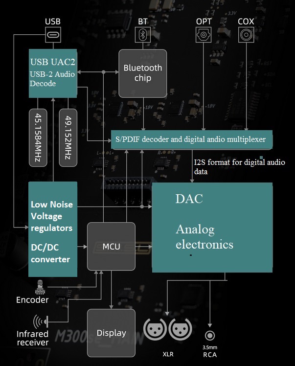
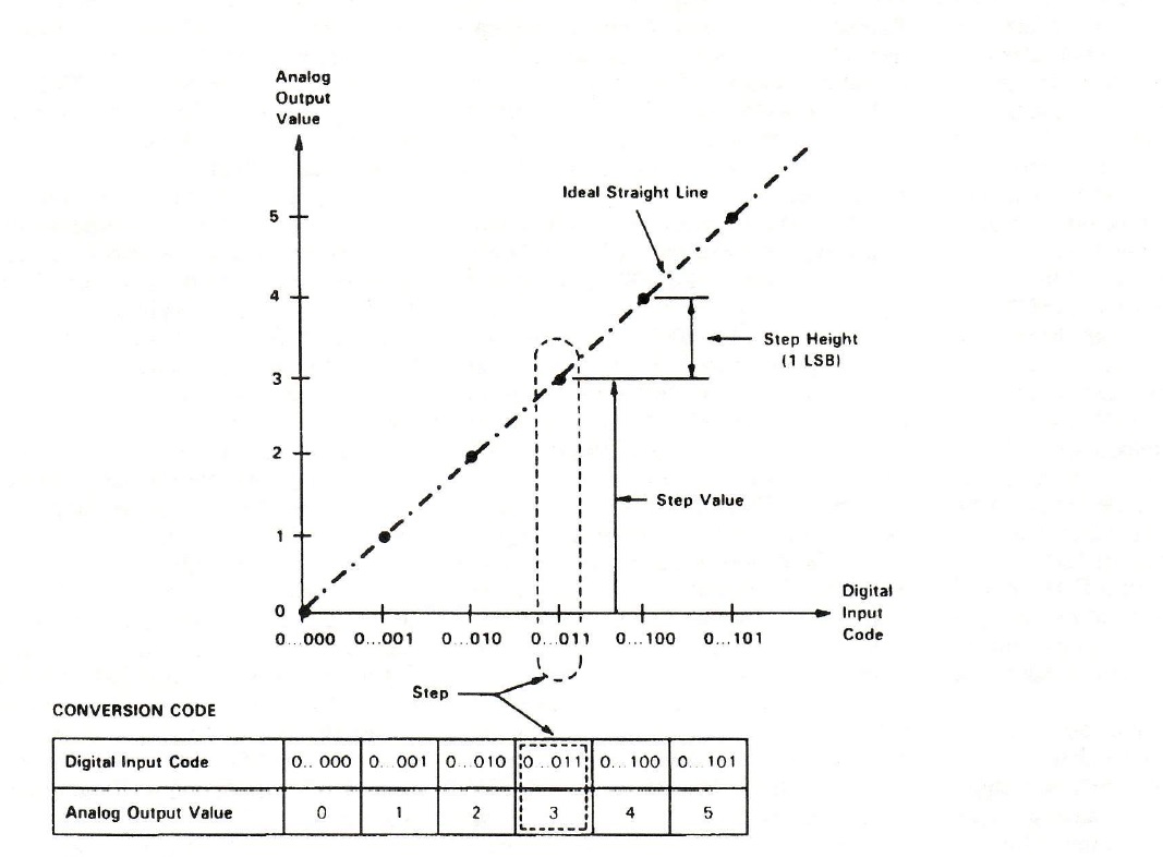
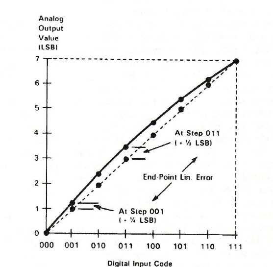
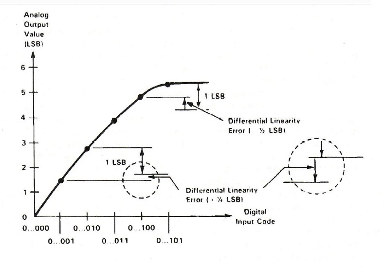
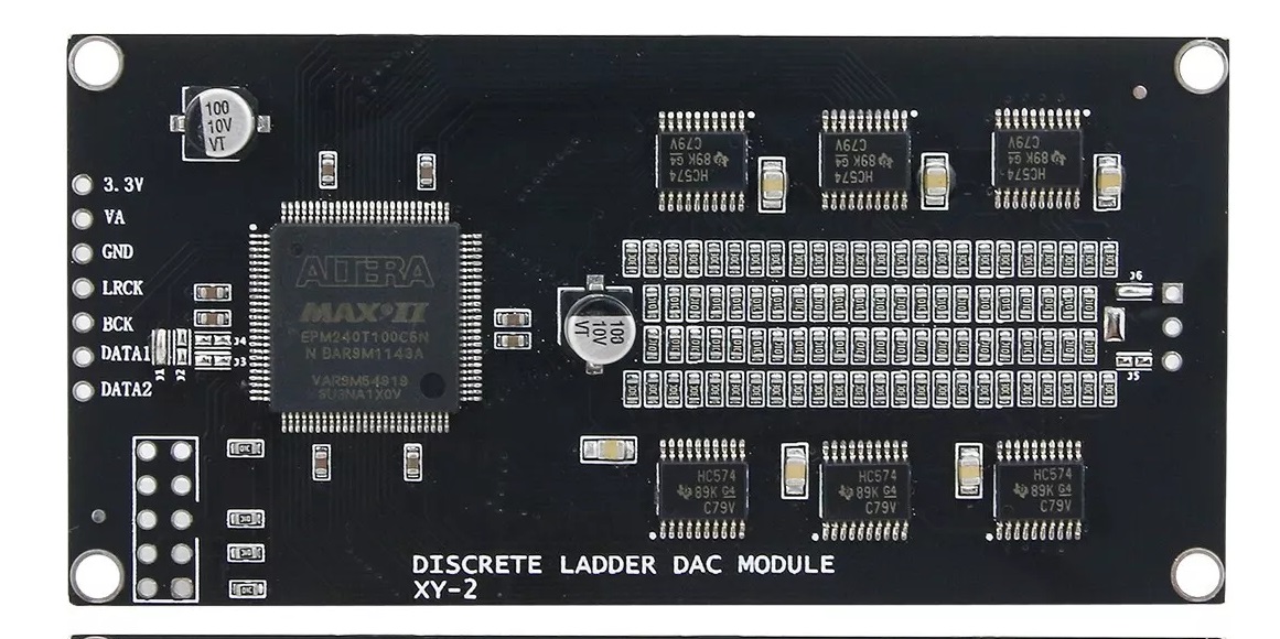
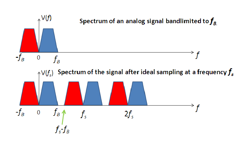
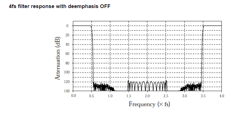
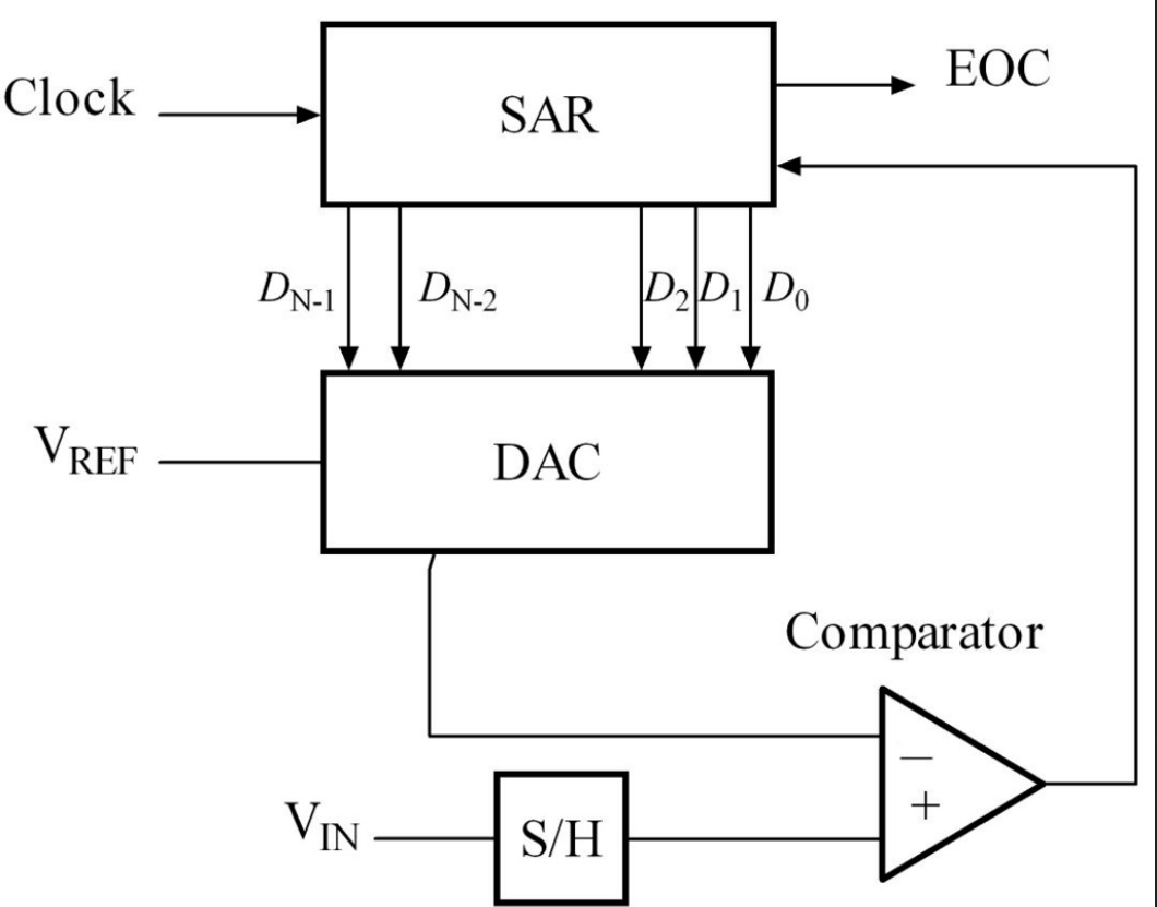
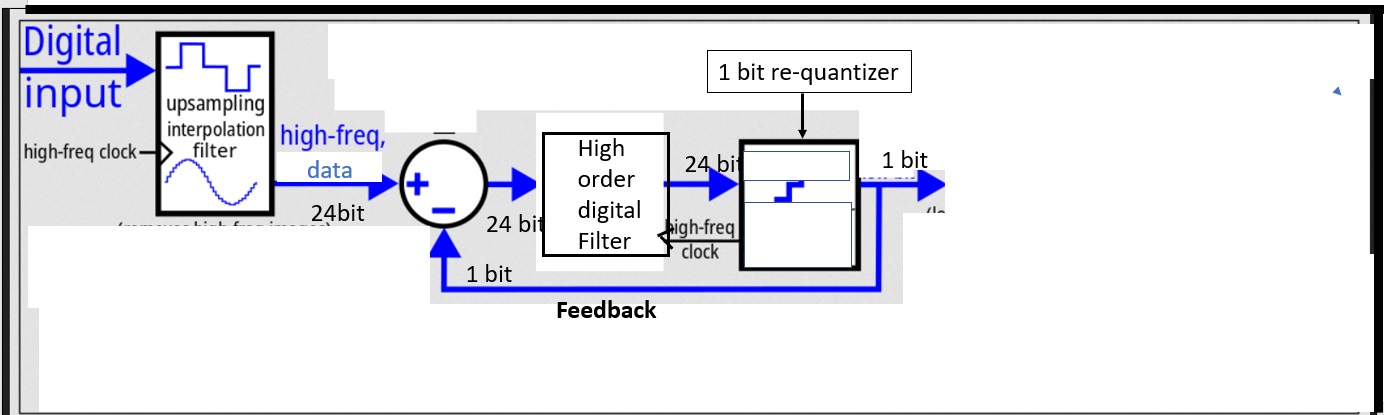
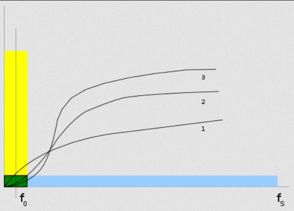
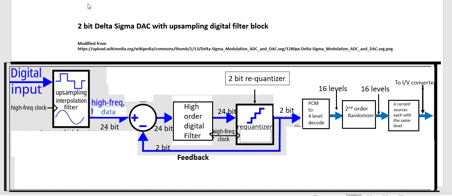
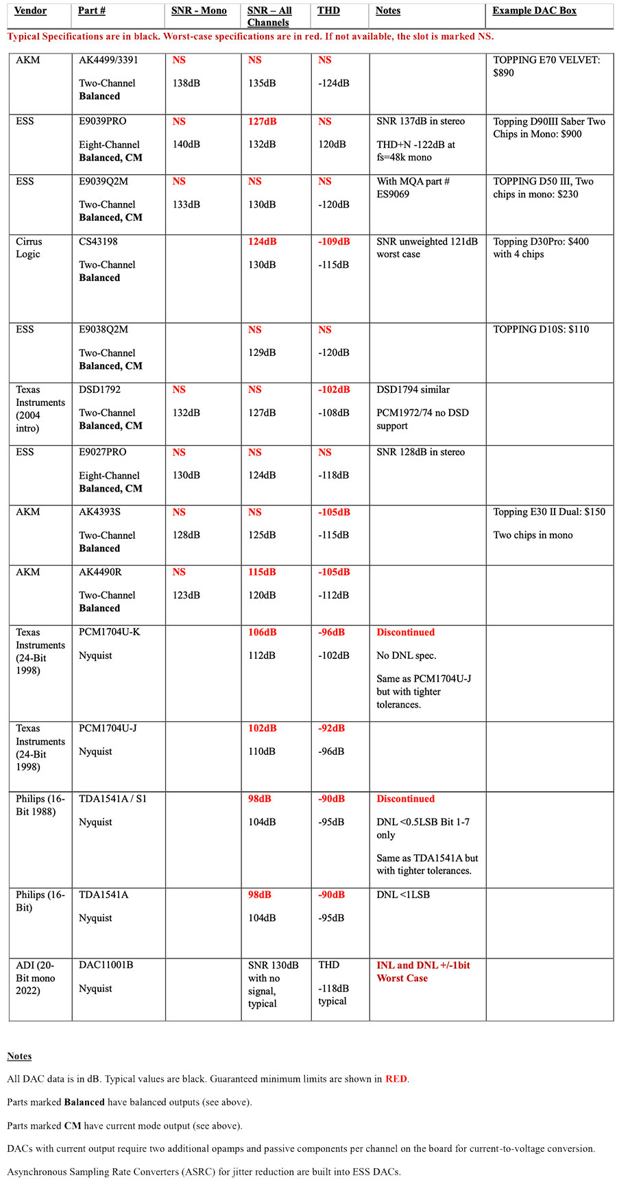
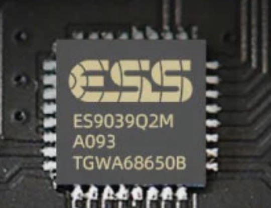
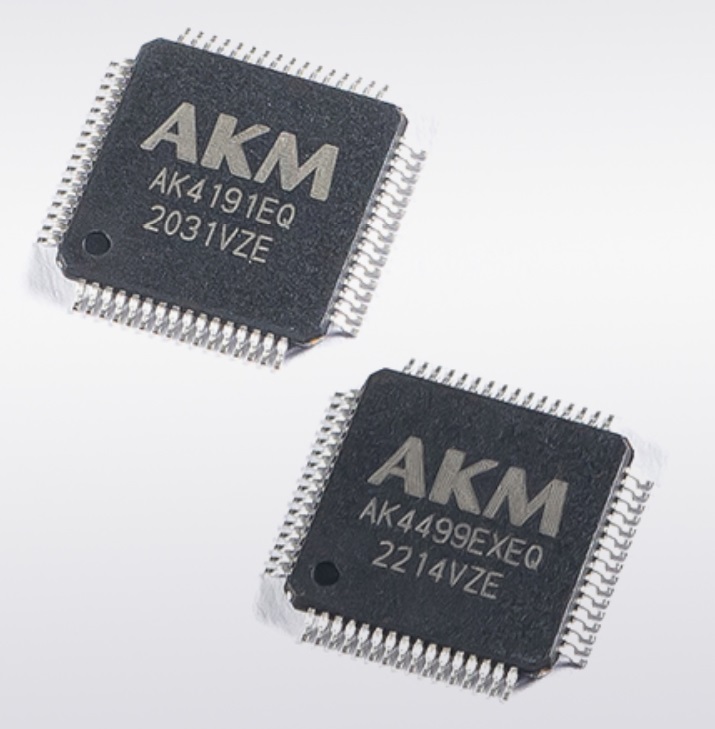
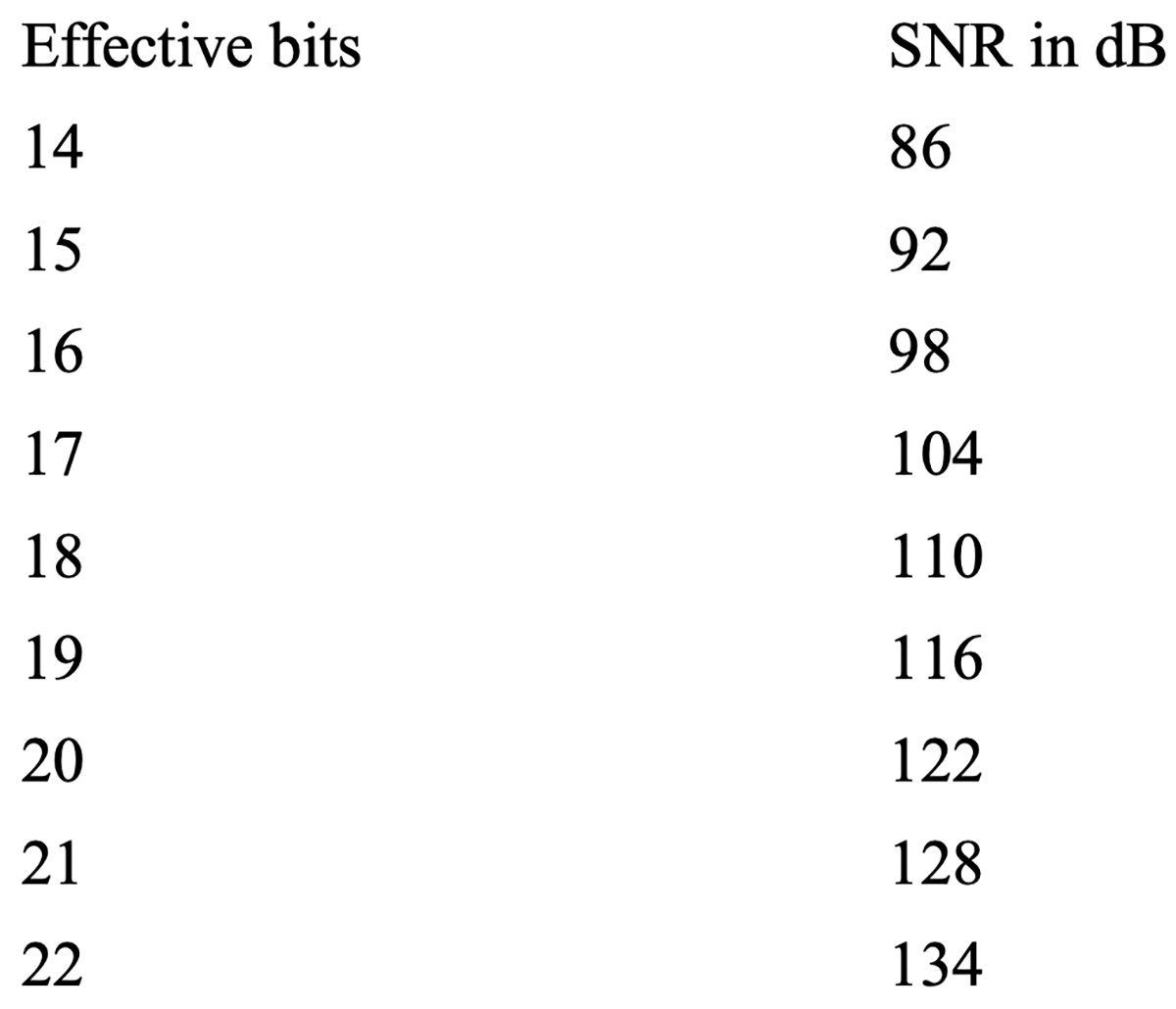
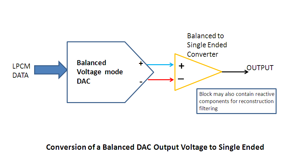
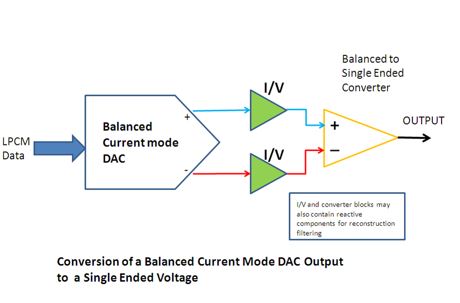
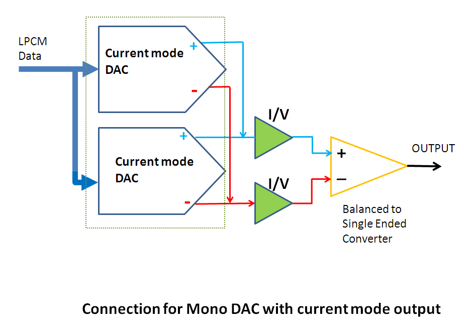
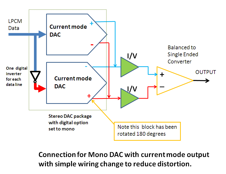
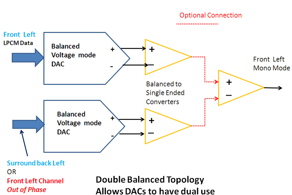
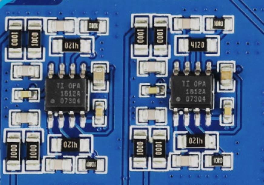
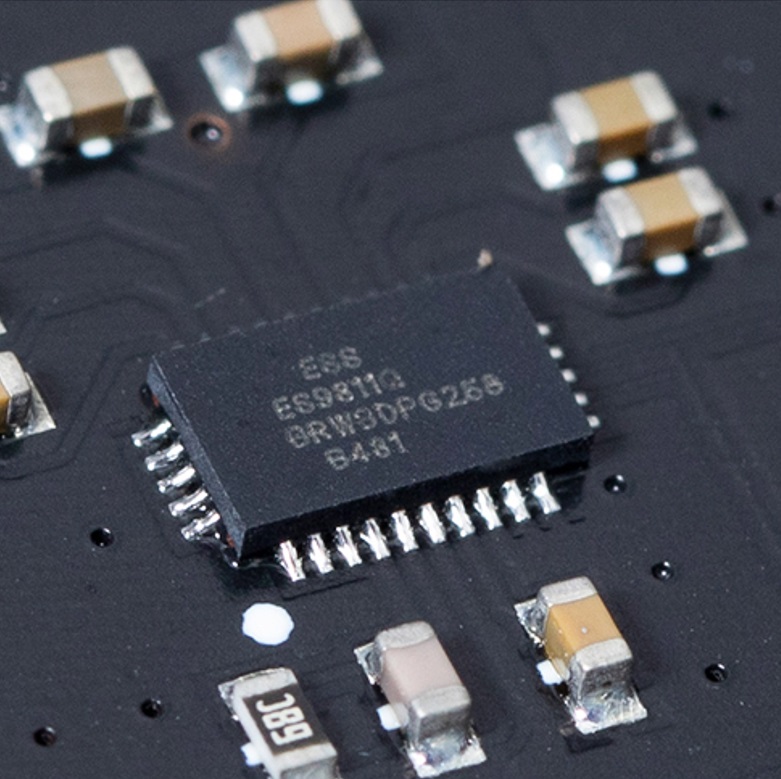