The ATI 6002 and Emotiva XPA-1 represent a major advance in amplifier designers. To my knowledge these are the first, high power, full balanced amplifiers with feedback from the input to the speaker terminal in high volume production. These amplifiers have significantly better performance when compared to bridged amplifiers as we will see below.
The two products are completely different designs. The Emotiva design will be discussed first. This design uses the inverting feedback topology. The ATI uses the non-inverting feedback topology which will be introduced later.
As we will see below, the fully balanced amplifier requires three feedback loops (networks) instead of the one in the standard amplifier. Each feedback loop can cause the amplifier to oscillate at its output. It is much more difficult to stabilize three feedback networks in comparison to one.
Fully balanced operational amplifiers (op-amps) are common in LSI chips. Stabilizing a power amplifier is much more difficult than stabilizing an operational amplifier since the loudspeaker load can vary significantly. The voltages and currents are significantly higher.
Current flow in the Inverting Amplifier
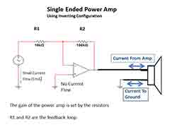
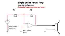
I have to go to the simple circuit level to outline the advantages of the full balanced amplifier and the challenges the designers face. We begin with a schematic (Figure 1) of a standard inverting, single ended, amplifier shown on the next slide. Most of you worked with this circuit in High School physics.
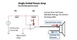
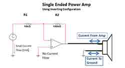
Figure 2 illustrates the current flow through the complete circuit when the + speaker terminal is at a positive potential.
When current is being driven into the + terminal of the speaker the current comes from the positive power supply and runs through the amplifier. The current then flows out of the speakers – terminal into ground
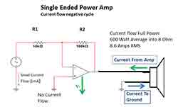
In Figure 3, we see the current flow through the complete circuit when the + speaker terminal is at a negative potential.
When current is being driven into the – terminal of the speaker the current comes from the ground terminal. The current flows out of the + speaker into the amplifier. The current then comes out the amplifier into the negative power supply.
When the speaker terminal is connected to ground, certain issues arise (Figure 4).
It can be seen above that three distinct grounds exist, one at the input, one at the pin on the power amp and the speaker ground. Single ended amplifiers have the disadvantage the current flows in the ground connections.
The ground does not have zero impedance so some signal must be at the negative terminal of the amplifier. All three grounds must be at the same potential not only at DC but also for AC signals If the grounds differ in potential distortion will be introduced. Special grounding techniques must be used to insure the grounds are all at the same potential.
Things become more complex because the power supplies are active for only half the signal cycle. The wave shape at the power supplies is identical to a half wave rectifier and power supply lines can radiate harmonics of the desired signal to the inputs and grounds inductively.
Self, D. Audio Amplifier Power Design, 6th ed. Focal Press, 2013, pp.288 – 295.
Developing a Fully Balanced Amplifier From a Single-Ended Inverting Amplifier
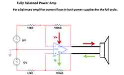
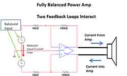
Figure 5 is a generic schematic for a fully balanced amplifier.
The power amp now has 5 terminals. The Vocm terminal will be explained later. The additional output Out- has been introduced at the power amp output and is in anti- phase with Out + output.
A balanced input has been used for this schematic.
Looking at the schematic you can see the balanced amplifier is made by copying and folding the single ended inverting amplifier. Note both the + and – inputs of the power amp are used. In the single ended inverting amplifier the + input of the power amp was connected to ground.
Two feedback loops are seen. The standard loop connected to Out + and a new connected to Out.
For an RCA single ended input a balanced to single ended converter may be used to maintain full balance in the power amplifier.
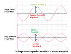
The voltage at the speaker terminals of the balanced amplifier is shown in Figure 6. It can be seen the speaker sees the same voltage from the speakers + to – terminals as a single ended amplifier.
Current flow in the Fully Balanced Amplifier
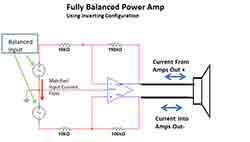
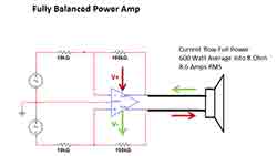
The current flow in the full balanced amplifier is shown in Figure 7, when driving current into the + input of the speaker. Note that both power supplies conduct current and no current flows in ground.
The current comes from the positive power supply and runs through the amplifier. The current comes out the Out + terminal of the amplifier to the speakers + terminal. The current flows out of the speakers – terminal into the amplifier Out – terminal and then down through the negative power supply.
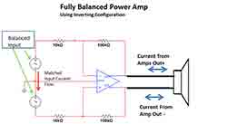
Figure 8 shows the current flow in the full balanced amplifier is shown when driving current into the – input of the speaker. Again note that both power supplies conduct current and no current flows in ground.
The current comes from the positive power supply and runs through the amplifier. The current comes out the Out – terminal of the amplifier to the speakers – terminal. The current flows out of the speaker + terminal into the amplifiers Out + terminal and then down through the negative power supply.
Note the current flow through the speaker is identical for the balanced and single ended amplifier if the same. The output transistors of each side of the amplifier must be designed to source and sink the same current level. For this reason the total number of output devices may increase in a balanced amplifier. The power dissipated by each output stage of the balanced amplifier is half of the power dissipated by the one output stage in a single ended amplifier.
In Figure 9, we consider the ground terminal in a balanced amplifier.
The balanced amplifier removes any current flow in ground from the speaker. In addition no ground is connected to the feedback components. If the input is balanced no current will flow in its ground pin.
Cordell, B. Audio Power Amplifiers. McGraw Hill, 2011, 527 – 535
Even Order Distortion Product Reduction in the Fully Balanced Amplifier
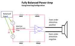
The balanced amplifier has reduced distortion compared to the single ended amplifier. This is shown in Figure 10.
In a balanced amplifier the even order distortion products at the Out + terminal are always the same positive polarity For the Out – terminal even order distortion products are always negative When combined at the speaker terminal the even order terms cancel in the ideal case.
Karki, J. “Fully-Differential Amplifiers.” Texas Instruments, Application Report
SLOA054D, 2002, p. 6
www.ti.com/lit/an/sloa054d/sloa054d.pdf
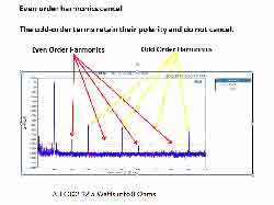
The plot in Figure 11 shows a spectra of a balanced amplifier taken across the speaker terminals.
ATI 6002 12.5 Watts average into 8 Ohms
Figure 12 illustrates another important attribute of the balanced amplifier.
Two feedback loops insure amp the amplifier operates in full balance The Out+ and Out- must be in exact anti-phase. If the signal level of Out + exceeds Out – this condition would be transmitted to the – and + input terminals of the amplifier by the two feedback loops and corrected.
The Bridged Amplifier and its Disadvantages
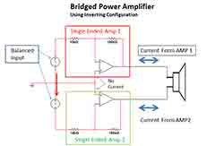
Figure 13 represents the schematic of a standard bridged power amplifier.
The bridged amplifier is driven by a balance input. Here two single amplifiers are used instead of one balanced amplifier.
The two bridged amplifiers do not match due to component production variations from the values printed on the capacitors and resistors. Transistors also vary between samples as can be seen from a data sheet.
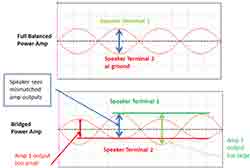
The effect on the voltage across the speaker is shown in Figure 14.
The amplifier output from Amp 1 is lower than what would be produced if all components had the nominal value. Amp 2 is producing too much voltage also as a result of the component variations.
For a balanced amplifier Out + and Out – must have the same potential as a result of the interaction of the coupled feedback loops. This applies even if the components of the amplifier vary from the nominal value.
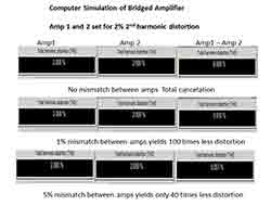
In Figure 15, a computer simulation is made for an ideal balanced amplifier and two bridged amplifiers with differences at the output of 1% and 5%.
In the simulation two amplifiers were created with 2% second harmonic distortion. This can be seen on the THD meter display of the computer simulation. The two amplifiers outputs are in anti-phase. The third THD meter shows the difference voltage between the two amplifiers. The performance degradation at the speaker terminals is clearly seen as the amplifier mismatch increases.
The reference below provides a more complete analysis of the effect of mismatch in a bridged amplifier:
Takahash, S. “Fully Balanced Bridge Amplifier.” Journal of the Audio Engineering Society Volume 32 Issue 6; June 1984 pp. 415-417
Common Mode Feedback
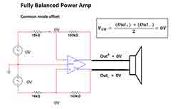
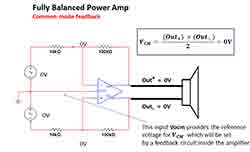
On the next schematic (Figure 16), an important concept of common mode level is introduced. This is a new concept specific to balanced amplifiers.
The common mode voltage is the sum of the two speaker terminal voltages divided by 2. The common mode voltage at the output should be 0V as shown above.
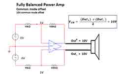
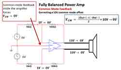
Figure 17 shows the common mode voltage at the output of the amplifier is 10V DC. The effect on the amplifier is discussed below the figure.
Above we can see the significant problem in balanced amplifier has that must be addressed. The two differential feedback loops cannot sense the common mode voltage of the speaker terminal.
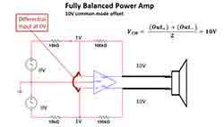
Figure 18 gives a deeper understanding of why the amplifier cannot see the common mode voltage on the output.
In this example the common mode voltage at the output is 10V. The resistor divider action of the two feedback loops sets the input to both sides of the amplifier input to 1V
The differential voltage across the amplifier input (in- – (in+)) is 0. The amplifier has no knowledge the common mode output is at 10V.
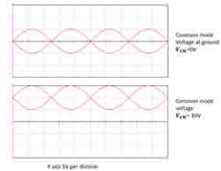
The computer simulation in Figure 19 indicates what the amplifier output looks like with a common mode voltage of 0V DC and 10 VDC
Without some method to control the common mode voltage the speaker outputs could move away from ground in tandem. The two differential feedback loops have no knowledge of this since they have no ground reference. The output in tandem would move to the positive or negative supply rail and the amp would stop working.
A third feedback loop to resolve the problem is shown in Figure 20.
The amplifier has 3 feedback loops not 2. The two differential feedback loops have been discussed above.
The third feedback loops sets the common mode voltage to 0V.
The circuit in Figure 21 has been annotated to show the action of the third common mode feedback loop.
The common mode feedback forces the average of the amplifiers output terminals to 0V.
The section below is more technical and you can skip to the next section.
A pair of identical resistors placed across the amplifier terminals will have the common mode voltage at the center point of the resistors. This is hidden inside the power amplifier symbol. An operational amplifier hidden in the power amp symbol compares this level to Vcom.
If the common mode level at the output is above Vcom the operational amplifiers output (inside the symbol block and not shown) increases in level. If the common mode level at the output is below Vcom the operational amplifier output decreases in level.
Typically the common mode feedback terminates at the differential pair tail current source which is again inside the power amp symbol and not shown. Increasing the current lowers both outputs until they are at ground. The voltage that controls the current source comes from the opamp inside the power amp symbol that is in the common mode feedback loop.
As can be seen the feedback is negative. When the common mode voltage goes up and so does the internal opamp voltage. This in turn increase the current in the current source connected to the differential which pulls the amplifiers outputs down.
A complete common feedback circuit is show in figure 2 of the reference below:
Karki, J. “Fully-Differential Amplifiers.” Texas Instruments, Application Report
SLOA054D, 2002, p. 6
www.ti.com/lit/an/sloa054d/sloa054d.pdf
Copyright restriction prevents me from showing the schematic here.
The figure also shows the complete amplifier with the two differential feedback loops in place.
Design Challenges in Production of the Fully Balanced Amplifier
If the common mode feedback loop goes unstable both amplifier outputs will oscillate in phase. If the differential mode feedback loops go unstable the amplifier outputs will oscillate out of phase.
The design of a power amplifier with three interacting feedback loops is very challenging in since the speaker load varies dramatically in resistance and reactance with frequency. The amplifier output is swinging large voltages and sourcing large values of current. This is in contrast to an opamp with a 10k Ohm resistive load and a +/- 15V power supplies.
Even if the amplifier is stable in normal use, an unexpected loss of power such as a thunderstorm can cause the amp to emit large pulses before it turns off. Shorting the output terminals for a second and then quickly removing the short can also cause instability.
Issues of stability are why fully balanced power amplifiers designs are often terminated before production.
Some designers cheat and run the feedback loop around the voltage amplification stage to isolate the feedback loops from the speaker load. The current gain stages that drive the speaker are open loop giving rise to significant distortion. More on the voltage and current blocks of a power amplifier is discussed below.
Design of a Low Noise, Fully Balanced Amplifier, with High Input Impedance
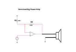
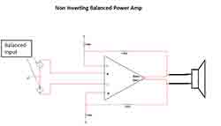
Up to this point the balanced amplifiers have been built on an inverting amplifier prototype. Another type of amplifier is called non-inverting, as demonstrated in Figure 22.
This is the standard topology for a power amplifier. This amplifier does not invert the incoming signal.
This amplifier topology has the advantage that the input impedance is very high since the input goes directly to the differential pair inside the power amp. The input resistance will typically exceed 100k Ohm.
R1 and R2 form the feedback network and set the amplifiers gain. R1 can be made small enough that it is not the primary source of amplifier noise. This is possible since the value of R1 is independent of the input impedance in the non-inverting configuration. Why the size of R1 changes the amplifiers noise is discussed below.
A typical single ended non-inverting amplifier, designed for low noise, would set R1 to 100 – 200 Ohms. At this value other sources of noise in the amplifier dominate. With this value of R1 and careful design to reduce other sources of noise in the power amp the SNR at full scale can be 125dB or more. This matches the SNR of the finest DACs available today.
The SNR can be very high, provided all the noise sources are addressed, since the power amp has large headroom. For 300Watts average the RMS voltage swing is 50VRMS Compared to the standard 2VRMS SNR reference normally used for SNR for the output of a digital source. The increase in SNR is 28dB.
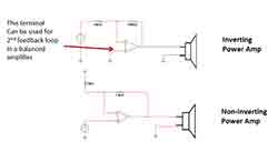
Here (Figure 23) are both the inverting and non-inverting single ended amplifiers.
Recall how we made a fully balanced amplifer from an single ended inverting amplifer by coping the amplifer and rotating the copy 180 degress. In the process the + termonal of the amplifer was removed from ground and connected to the secound differential feedback loop. The only change to the power amp was the need to build in the circuitry to produce the anti-phase Out – terminal.
It is not easy to create a balanced amplifier from the non inverting topology since both the + and – inputs have signals attached.
The schematic in Figure 24 suggests that we need to make significantly more changes to the power amp than just adding an Out – terminal and its associated circuitry.
The amplifier must be modified so that it has duplicate differential inputs. As can be seen above the amplifier has two + inputs and two – inputs. This introduces significant design challenges.
The remainder of this section is technical and you can go to the next section.
One approach, common in integrated circuits, is to use two differential pairs. One for the balanced input and one for the feedback. This requires extremely close matching of the two differential pairs since the differential pair connected to the balanced inputs is out the feedback loop.
Special IC layout techniques may be used to reduce mismatch between the circuits. Circuit designs used inside an integrated circuit cannot be applied to a discrete amplifier since the component variations are too large.
A novel approach is to use one differential pair. The balanced inputs are connected to the base connections of the differential pair. The feedback is current mode and the summing junction is the emitters of the differential pair.
This approach was disclosed in the paper below.
Bongiorno, J. “Ampzilla III” The Audio Amateur 15.4 (September 1984): 7 – 19
The magazine is hard to get now but is often available on eBay.
Note that the current feedback in Bongiorno paper is done differently then what is done in integrated circuits that use current feedback. Again the IC technique requires extremely good matching between devices.
Many power amp manufactures have tried to copy the IC based current feedback stage with discrete components for single ended power amps but it is always suboptimal. Copying the ICs schematic with very closely matched transistors and replacing then with discrete components creates more problems then it fixes.
Self, D. Audio Power Amplifier Design, 6th ed. Focal Press, 2013 pp 213 – 215.
It is not well known but before the differential pair came into wide use in audio circuits current mode feedback was commonly used. The summing node was the emitter of a single transistor at the front end of the amp. The input was at the base of the one transistor.
The problem was a DC offset was introduced between the base and emitter which was difficult to deal with and still produce a DC coupled amp.
Self, D. Audio Power Amplifier Design, 6th ed. Focal Press, 2013 Figure 30.6.
Note the capacitor between the amps’ output and the speaker terminal.
This single transistor circuit is the differential mode half circuit for the Bongiorno balanced power amplifier core disclosed in the above paper. The offset is removed using a complementary circuit approach which will be discussed below.
Although the Bongiorno paper above was a DIY project I do not know if one was successfully implemented. Note the very complex DC offset correction used to set the common mode and differential mode offsets to 0. Also note the many compensation capacitors that have a function the is not easily understood. Other land mines are also present.
Noise in the Single-Ended Inverting Power Amp
For ease of reference, here is the same figure as at the beginning of this article: the single ended inverting amplifier.
The input resistance of the power amplifier is set by R1
Rin = R1
In an audio amplifier it is desired that the input impedance be as high as possible to reduce the load on the preamp output stage but we have another design issue to contend with when picking R1.
All resistors produce noise generated by the thermal agitation of electrons independent of any applied voltage. The smaller the resistor the less the noise.
www.sengpielaudio.com/calculator-noise.htm
It can be shown the size of R1 sets the output noise of the amplifier if R1 exceeds a value specific to the amplifiers internal design.
A tradeoff exists between the noise of the amplifier and its input resistance The current noise from the bipolar transistors in differential pair enhances the change in the noise as the value of R1 is increased.
Self, D. Audio Power Amplifier Design, 6th ed. Focal Press, 2013. pp150 -157
These issues can be resolved using a unit gain buffer before the amplifier. The buffer provides a high impedance input for the preamp and can drive a 100 Ohm resistor. If 100 Ohms was selected for R1 the noise in the amplifier would be dominated by other electronic components.
For a balanced inverting amplifier a pair of buffers can be used to solve the issues of achieving high input impedance and low noise. The buffers must be single ended. A low distortion, low noise, balanced input buffer is not easily designed. Indeed it has the same problems as a balanced non-inverting power amp. The lower signal voltages in the input buffer produce much less distortion. A fully balanced approach for the buffer provides no real advantage.
A More Detailed Look Inside the Single-Ended Non-Inverting Power Amp
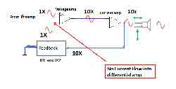
Below (Figure 26), I show the non-inverting feedback amplifier with the internals of the power amp shown in more detail.
It can be seen the amplifier is divided into two parts. A differential voltage amplifier which increases the size of the signal and a current amplifier which drives the speaker but does not increase the signal size.
In a power amplifier the voltage amplifier may have two stages and the current amplifier has two or three stages.
The voltage across the differential amplifier must be 0. This condition forces the input and midpoint of the feedback network to the same amplitude. If the feedback network, which is composed of two resistors, attenuates the signal by 10 the output will be 10 times the input signal.
Note the red arrow points to the – terminal. This negation makes this negative feedback. The figure shows the differential voltage amplifier has a very high input impedance. No current flow in the – input so all the current flowing in the feedback loop goes to ground.
Complementary Circuit Design for Reduced Even-Ordered Distortion
It is desired to reduce the distortion as much as possible before the feedback is applied so the closed loop distortion numbers are very low. Alternatively the amplifier can be designed to have lower open loop gain across the audio band.
One way to lower the distortion open loop is to use complementary circuits. This is also called push-pull. The technique reduces even order harmonic
http://en.wikipedia.org/wiki/Push%E2%80%93pull_output
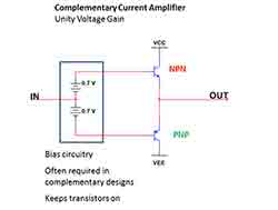
This schematic (Figure 27) shows a complementary voltage buffer with current gain. This circuit is found at the output of most op-amps.
In a complementary design every PNP transistor is matched by an NPN transistor for the entire circuit. A complementary current amplifier such as the one shown above is almost always used for the output stage of a power amplifier. In a power amp two or three stages of complementary current amplifiers are used.
The schematic shown in the reference below is for a 3 stage current amplifier in cascade. Such a circuit is mandatory for an amplifier designed to drive 400 Watts average into 4 Ohms.
Self, D. Audio Power Amplifier Design, 6th ed. Focal Press, 2013. Figure 10.13
Moving from the +/-15Volt power supply of an opamp to the +/-70 Volt of a power amp (this voltage is used for amps rated 300 Watts average into 8 Ohms) results in a significant increase of in distortion in the voltage gain stage proceeding the current gain stage. Most large power amplifiers are completely complementary including the voltage gain stage. Lower power amplifiers in AVRs are often complementary only in the current gain stages that drive the speaker. This is not a disadvantage for power amps below 150 Watts into 8 Ohms.
Self, D. Audio Power Amplifier Design, 6th ed. Focal Press, 2013 Pages 216 -217
Complementary circuits and balanced amplifiers reduce even order distortion. To reduce open loop odd order distortion in the amplifier other issues must be addressed such as the linearity of the differential pair and crossover distortion.
The next section looks at Class A biasing as a method to reduce even order and odd order distortion. Optimal Class AB biasing will do almost as well with a significant reduction is standing power dissipation.
Power Dissipation of a Class A Amplifier
The Class A output stage removes crossover distortion by keeping both the pull-up and pull down transistors on for the full voltage swing at the output. This prevents crossover distortion since the output transistors never crossover.
Self, D. Audio Power Amplifier Design, 6th ed. Focal Press, 2013. 424 – 429
The problem with the Class A amplifier is it dissipates more current with no signal then when it is driving the speaker. Dealing with the implication of this issue significantly increases the amplifier cost.
To make the calculations in this section simpler I am going to use a single ended amplifier. Note the power output to the speaker is always average. RMS power does not exist. Standing power dissipation is DC Watts.
A single ended 200 Watt average amplifier swings 40VRMS (56V Peak) and sources 5 Amps RMS (7 Amps peak). A single ended 200 watt average amplifier (40VRMS * 4Amps RMS) is designed to stay in Class A for the full voltage sources 7.0 Amps DC to the speaker before the before one of the transistors turns off.
For a 200 Watt average amplifier the power supplies are slightly larger than the peak voltage swings at about +/-60V DC.
In a Class A amplifier the standing power dissipation is half of the maximum current the amp can source to the loudspeaker before one of the transistors turns off.
3.5(60V – (-60V)) = 420 Watts.
An amplifier that can run in Class A for 200 Watts average into 8 Ohms can run 100 Watts average into 4 Ohms. Above 100 Watts average into 4 Ohms the amplifier will transition to Class B and one of the transistors will turn off.
The power dissipation of a Class A amplifier declines significantly if the power output is limited. Consider a 30 Watt average Class A amplifier into 8 Ohms. The amp swings 15.5VRMS (21V peak) and sources 1.9Amps RMS (2.7 Amps peak). The power supply rails for a 30 Watt average amplifier are about +/- 23VDC.
The standing current of a 30 Watt average class A is half the peak current at 1.35 Amps DC.
The standing power dissipation of the 30 Watt average Class A amplifier is calculated as:
1.35 amps (30V – (-30V)) = 81 Watts.
For a higher power amplifier the designer can choose to set the standing current of the amplifier lower so the amplifier only runs in class A to a specific power output and then transition to Class B. A 200 Watt average amplifier that stays in Class A for 30 Watts average and then transitions into Class B still has a standing current of 1.35 Amps. This was calculated above for the 30 Watt average Class A amp.
The power supply rail on the other hand for the 200 Watt average amp remains at +/-60V DC
The standing power dissipation for the amplifier is:
1.35 amps (60V – (-60V)) = 162 Watts.
This is 2.3 times less than the full 200 Watt average Class A amplifier which was shown above to dissipate 420 Watts of energy with no signal. Note dropping the Class A transition power by a factor of 6.8 to 30 Watts average has not reduced the static dissipation by anywhere near the same amount. Indeed it can be shown the dissipation declined be the square root of the change in the Class A transition power.
The next two sections are technical and you can go to the conclusion.
Stabilizing the Output Transistors’ Standing Current for a Class A Amplifier
To set the current in the complementary output stage we need to add a resistor is series with each output transistor.
Below (Figure 28) the placement of the resistor is shown:
To stabilize a Class A stage the voltage across the resistor in series with the output transistor must be made significantly larger than the transistors VBE change over the full current swing.
Let us return to the 30 Watt average Class A amplifier discussed above which simplifies this discussion compared to the 200 Watt amplifier with a transition from Class A to B at 30 Watts amplifier. The standing current for the 30 Watt Class A amplifier was calculated as 1.35Amp.
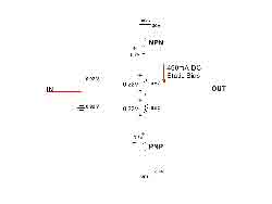
To deal with the high standing power dissipation in the transistors 3 parallel output might be used. Each transistor must dissipate 450mA of standing current (1.35 / 3). Since the power amp rails are +/-30VDC the transistors can have a lower rated breakdown voltage.
We do not want the resistor to be so large that is dissipates significant power that could go to the load. For the example in Figure 28 above, I used a 0.5 Ohm resistor which produced a 22mV when 450mA flows through it. This voltage is well above the change in VBE from no signal to near the edge of Class A operation. This achieves the design goals.
Note this is one of 3 output transistor groups in parallel. The three paralleled 0.5 Ohm resistors thus have an effective output resistance of 0.17 Ohm before feedback.
Sub-optimal Class A/B Operation when a Simple Switch is used to Change from Class A to Class A/B
Returning to the 200 Watt average amplifier Class A. We calculated a standing power dissipation of 420 Watts above. We might want an option to switch to Class AB to lower this dissipation at the cost of more distortion.
The optimal bias for a class AB amp is one that minimizes the gain change of the current amplifier stage in the crossover region around 0V. The is achieved the emitter resistor in series with each transistor is approximately 100m -200m Ohm. For a given resistor value an optimum bias current can be calculated.
Self, D. Audio Power Amplifier Design, 6th ed. Focal Press, 2013 pp 277 -279.
The power output of the amplifier does not change the emitter resistor size or bias current for optimizing crossover distortion in a Class AB amplifier. Crossover distortion occurs over the same small voltage swing around ground regardless of the supply rails.
Our Class A design needed a 500m Ohm resistor to stabilize the Class A bias. This is too high for optimal Class AB operation. Crossover distortion will be higher as a result as can be seen in the figure in this text.
Self, D. Audio Power Amplifier Design, 6th ed. Focal Press, 2013. p 277 figure 10.30
It is possible to design an amplifier for optimal performance in Class A and Class AB operation. For optimal Class AB distortion the 100m – 200m Ohm resistor is placed in series with the emitter and a fixed bias is across the bases (changing with temperature). For class A operation a low cost added circuit.
In Class A operation the circuit measures the very small voltage across the emitter resistors and compares it to the voltage required to set the Class A standing current. If the voltage is too small the circuit increases the base spreading voltage (the batteries in the figure above). The circuit does the reverse and lowers the base spreading voltage if the current is too large.
Self, D. Audio Power Amplifier Design, 6th ed. Focal Press, 2013 pp 430 – 431.
If the amplifier enters class B at some point in the swing the Class A control circuit shuts off.
From the audiophile prospective this added active current control may be thought to degrade the transparency of the output stage although this can not be justified in objective measurements.
Conclusions
In this article I have highlighted the problems associated with single ended amplifiers and shown how these can issues can be removed by using a fully balanced design.
I showed that a bridged amplifier does not perform as well as a fully balanced amplifier. Common mode feedback was identified as the most significant design challenge for a fully balanced amplifier.
Two fully balanced amplifiers topologies were introduced. The inverting topology is simpler to design but will introduce will have higher noise or lower input impedance than a single ended topology. These issues can be resolved using a unit gain buffer before the amplifier.
The non-inverting balanced topology was the second balanced amplifier topology discussed. It does not require the additional buffer stage for good performance but the internal design of the amplifier is significantly more complex.
Additional topics on power amplifier design were also presented including advantages of complementary amplifiers and power amplifier output stage design. In addition this article discussed the calculation of standing power of a Class A amplifiers, thermal noise and the impact of thermal noise on SNR.
We discussed how using a simple bias switch change from Class A to Class AB operation yields sun-optimal Class AB performance and discussed how to correct this with simple added circuit.
The reader is now in a better position to understand the design tradeoffs of an individual product under review. I will highlight these in the measurement sections.


